Date:2024-06-11 11:35:07 Views:1250
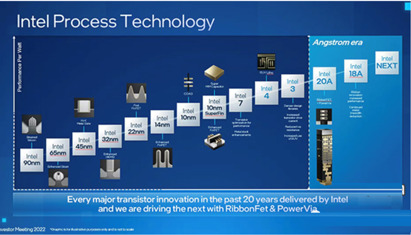
Intel in the U.S.A. is stepping up the development of the cutting-edge semiconductor "Intel 20A", the A in 20A meaning "angstrom". An angstrom is a unit of length that represents one-tenth of a nanometer, and 20A refers to 2 nanometers. Intel has proposed a new technology index in an attempt to reverse its disadvantage in the competition with TSMC and Samsung Electronics.
Currently, the metric for measuring cutting-edge semiconductor technology generally uses nanometers. Specifically refers to the line width of semiconductor circuits, the thinner the circuit the higher the processing power and data storage capacity of the semiconductor, but also able to curb power consumption and contribute to the miniaturization of semiconductor wafers. Semiconductor manufacturers have been competing to promote "circuit miniaturization" that is full of benefits.

Looking back at the history of large-scale integrated circuits (LSIs), Intel's Intel 4004, launched in 1971, was the starting point. At that time, the line width was about 10 microns, which translates into 10,000 nanometers. Since then, microfabrication has been achieved in accordance with Moore's Law, which states that the performance per unit area of a semiconductor chip doubles in about two years.
Without this innovation in semiconductor technology, IT products such as smartphones would not have been created. Today, semiconductors drive the evolution of all industrial products such as automobiles, white goods, robots, and industrial machinery.
The current state-of-the-art is the 3-nanometer semiconductor to be mass-produced by TSMC and Samsung. In contrast, Intel's latest technology is 7 nm. In the second half of the 2010s, Intel lagged behind in the development of production technology and was left behind.
Can such Intel make the leap to 20A, or 2-nanometer technology? The answer is no. One thing that should not be overlooked is that Intel does not explicitly state that "20A" refers to the width of the circuit line.
In fact, 5nm, 3nm, and other metrics have been diverging from the actual dimensions of circuit line width for about five years now. At present, there is no international standard on where to measure semiconductor circuits, and 3nm, which is being mass-produced by TSMC and Samsung, is just "corporate talk" (executives of semiconductor design companies).
Intel declared "the coming of the era of the emi" without specifying the unit of length. It is just a marketing slogan to show the advanced image.
So, what does line width refer to now? It is usually calculated by comparing the number of semiconductor components per unit area with its own products in the past, based on how many components have been added.
Although it is often used because it is simple and easy to understand, performance comparisons cannot be made simply by using this value. It is also necessary to focus on actual data processing power, data storage capacity, power saving performance, order quantity, etc.