Date:2023-11-07 11:37:48 Views:1151
Recently, Diamond Foundry Inc, headquartered in San Francisco, California, fabricated the world's first single-crystal diamond wafer with a diameter of 100 millimeters.
The company plans to offer diamond substrates as a way to improve thermal performance, which in turn could improve artificial intelligence computing and wireless communications, as well as smaller power electronics.

The company uses a process called heterogeneous epitaxy to deposit carbon atoms and fabricate single-crystal diamond on scalable substrates. Diamond wafers have been produced before, but they were based on compressed diamond powder and lacked the properties of single-crystal diamond.
Diamond Foundry says its next goal is to reduce the defect density of diamond wafers to achieve a quality factor 17,200 times higher than silicon and 60 times higher than silicon carbide.
Diamond Foundry operates a diamond and wafer production facility in Washington state.
Founded in 2012, the company operates in the jewelry and luxury markets as well as the semiconductor industry. The company says on its Linkedin site that it has secured $515 million in financing and is executing a multibillion-dollar expansion plan to convert greenhouse gases into diamond wafers using zero-emission energy.
According to them, the company can achieve the ultimate hot chip package by bonding diamond atomically to integrated circuit (IC) wafers thinned with angstrom-level precision.

Thermally, no other material conducts heat as efficiently as single-crystal diamond, resulting in chips that run faster and last longer. This allows the diamond wafer to provide a thermal highway within atomic distance of the working chip transistor. It dissipates heat with ideal efficiency, reducing hot spots and tripling the chip's computational speed.
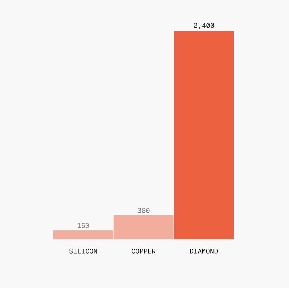
It is also an extreme electrical insulator, with the thinnest slices of diamond isolating very high voltages, enabling new levels of miniaturization in power electronics.
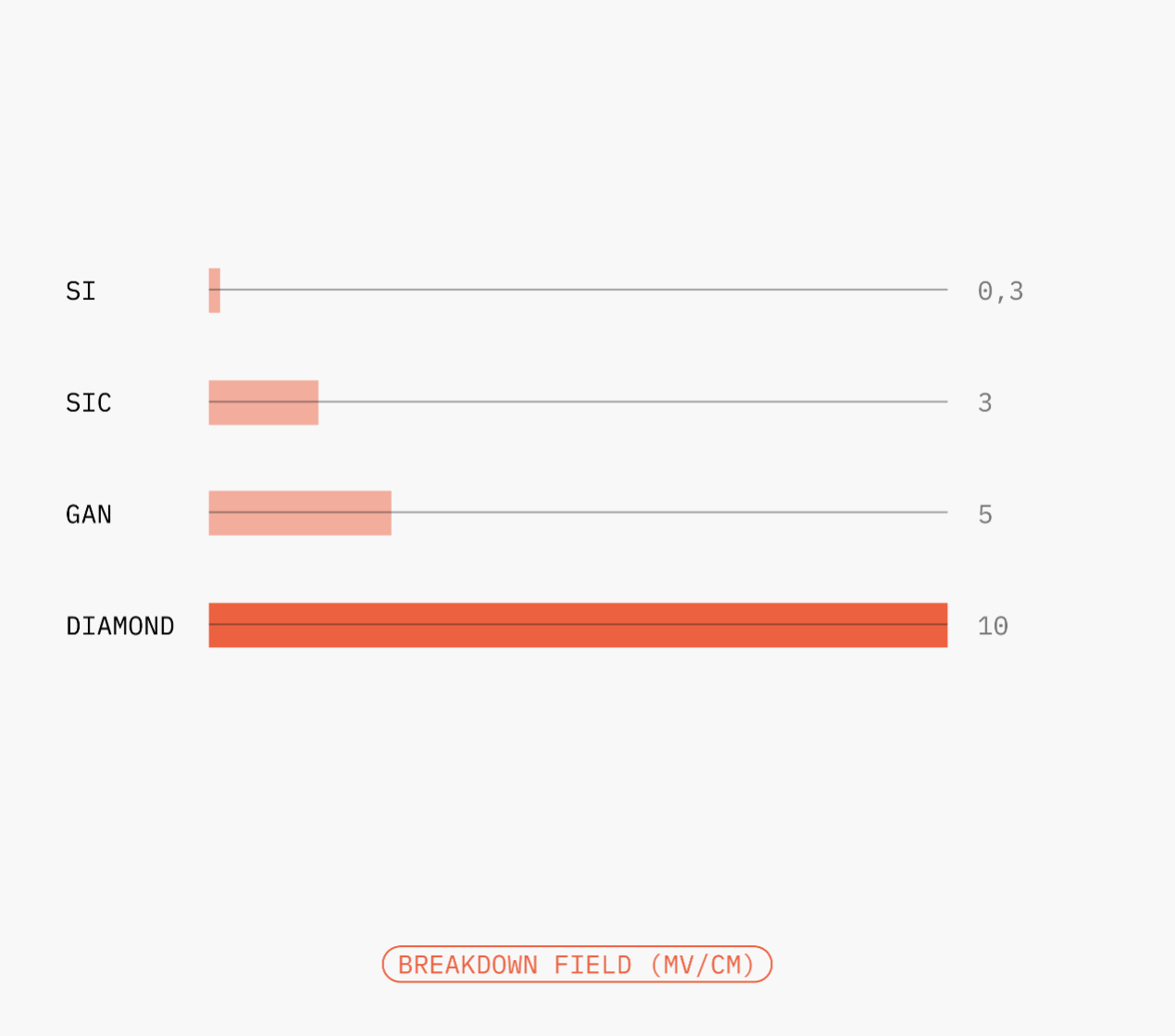
Thanks to these leading-edge features, Diamond Foundry believes the company's solution is suitable for all leading high-power chips. The combination of proven silicon chips and diamond semiconductor substrates dramatically accelerates cloud and AI computing, meaning the same performance can be achieved using half the space of a data center.
These advantages also allow it to simplify inverter design, as the extreme thermal conductivity and electrical insulation properties of diamond wafers allow the novel architecture to radically advance miniaturization, efficiency and robustness.
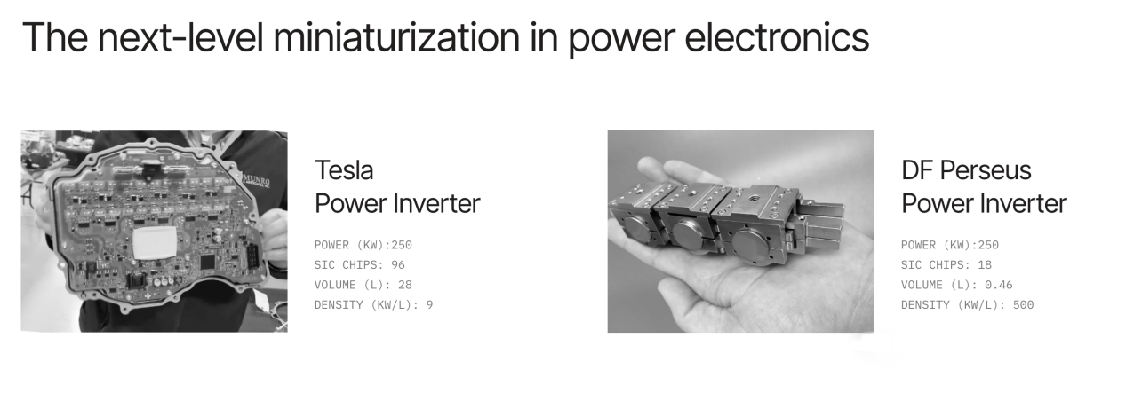
This leading-edge design also allows it to help in the field of wireless communications.
GaN semiconductors are said to power a growing number of the most efficient wireless communications. However, diamond wafers address overheating and voltage issues, making GaN superior to SiC in every metric.
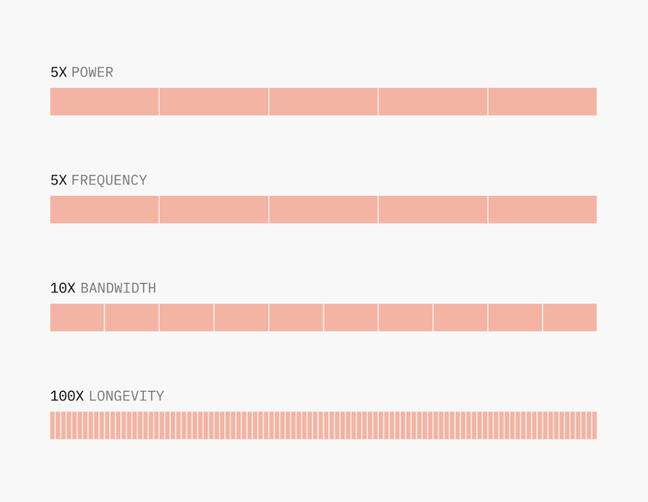
And the power density of diamond-based GaN MOSFETs is three times that of GaN without diamond. Reliability is improved by reducing thermal stress and interconnecting GaN atoms to DF (Diamond Foundry) single-crystal diamond.
A similar company, Diamfab SA (Grenoble, France), was founded in Europe in 2019.Diamfab synthesizes and dopes diamond epitaxial layers grown on other substrates with a view to fabricating superior power devices from diamond."