Date:2023-07-17 11:44:26 Views:1091
Materials are often known for specific advantages. Diamond has crucial applications in high power, high frequency, and high temperature fields precisely because of its highest thermal conductivity at room temperature (2000 W/m.K), combined with superior properties such as wide band gap, high breakdown field strength, high carrier mobility, high temperature resistance, resistance to acids and alkalis, corrosion, and irradiation. Diamond, has been recognized as one of the most promising wide-band semiconductor materials.
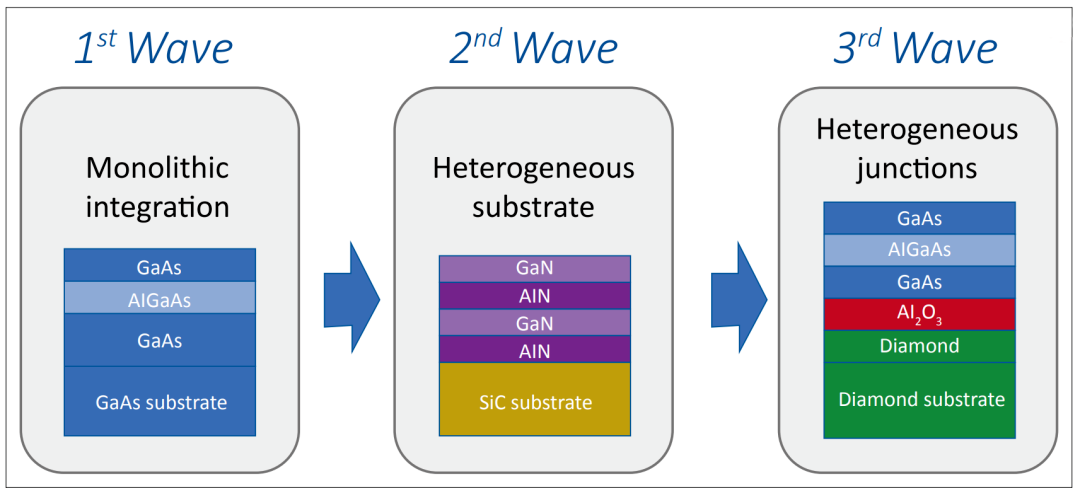
Mark Rosker, director of the Microsystems Technology Office at the U.S. Defense Advanced Research Projects Agency (DARPA), said at CS Mantech last year that the compound semiconductor industry will soon enter the third wave of materials technology. This era will see devices made from a combination of different materials.

Figure 1.According to Rosker, the third wave is now beginning to emerge, with devices using mutant junctions and high-performance materials with different lattice constants.
To illustrate what the third wave of devices might look like, Rosker highlighted a new type of HBT device innovated by a collaboration between the University of Wisconsin-Madison and Michigan State University. Using AlGaAs/GaAs film transfers grown on a homogeneous substrate, the team constructed HBTs with a diamond substrate, a p-type diamond collector, an Al2O3 interlayer, and AlGaAs layers that provide the emitter and base junctions (see Figure 1). By employing the grafting technique, the engineers overcame a 37% lattice mismatch between the GaAs substrate and the diamond. This is a breakthrough that opens the door to combining some of the traditional benefits of HBTs with diamond's excellent heat dissipation and higher bandgap for increased transistor breakdown voltage.

A more established method of combining different compound semiconductor materials is direct wafer bonding. A variant of this method, called surface-activated bonding, is attractive because it does not require any wet processing and the wafers are bonded together at room temperature.
Akash was a pioneer in diamond-based GaN, and to bond the materials together with this technique, the wafers are loaded into a vacuum chamber, which is pumped down to about 10-6 Pa. The wafer surfaces are then bombarded with a neutral beam of atoms (usually argon), which are accelerated by 1-2 kV. These collisions eliminate natural oxides and produce an activated surface. Pairs of wafers are then pressed together, usually at a bonding pressure of about 10 MPa (see Figure 2).

Figure 2. Working under vacuum, bombarding the wafers with a fast atom beam (FAB) removes the native oxide and creates a surface for bonding.
At CS Mantech, Naoteru Shigekawa, a group leader at Osaka City University and an expert in this type of wafer bonding, outlined the criteria for optimizing the process and then illustrated its capabilities with examples of novel devices. While his device is limited to joining wafers up to 2 inches in diameter, he was quick to point out that there are commercially available tools for high-throughput bonding of 300-mm wafers.
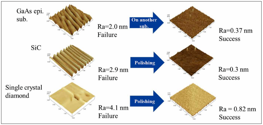
Shigekawa told attendees that the surface roughness of a wafer affects bonding yields. His team's experiments have shown that for bonding to be successful, the surface roughness value, Ra, must be less than 1 nm, ideally less than half that value. Epitaxial wafers tend to be well above this value, but polishing flattens their surfaces for successful bonding (see Figure 3).

Figure 3. The flatness of the wafer determines bond yield. Polishing reduces roughness and increases the chances of high quality bonding.
Care needs to be taken when applying this form of bonding because surface activation can lead to dry etching, which increases surface roughness and reduces yield. Another disadvantage of etching is that it introduces an intermediate gap state. "We hypothesize that this intermediate gap state has a negative impact on the electrical properties of the bonded interface," says Shigekawa, who adds that one solution is post-bond annealing, which can lead to recovery of the interface properties.
To illustrate this point, Shigekawa showed transmission electron microscopy of bonded silicon and GaAs wafers. Before annealing, there is an amorphous-like transition layer at the interface. Annealing at 300°C causes the layer to shrink, while at 400°C it disappears due to recrystallization.
Shigekawa and colleagues also used electrical measurements to assess how annealing adjusts interfacial properties. Studies of junctions formed by bonding two n-type silicon wafers together, as well as by bonding two p-type silicon wafers together, showed that annealing at 1,000°C for 10 minutes reduced the interfacial density of states from around 1013cm-2eV-1 to one-fifth of this value.
The Osaka City University team has produced a range of novel devices with wafer bonding, including multi-junction solar cells, power devices with junctions between wide and narrow bandgap materials, and field effect transistors with a diamond layer to increase current diffusion. For the latter, the devices are formed by bonding diamond directly to semiconductor materials, one being silicon and the other GaA, and bonding the diamond to a heat sink. The new architecture promises to dramatically reduce thermal resistance.
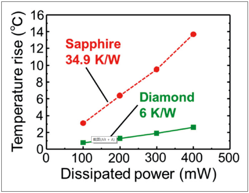
Using a thermal imager, Shigekawa and coworkers measured the thermal resistance of their junctions. To provide a benchmark, they used a bonded GaAs-sapphire junction with a thermal resistance of 35 K/W (see Figure 4). In comparison, the GaAs-diamond junction has a resistance of only 6 K/W, which allows the device to operate more consistently and reliably without overheating, or to employ simpler thermal management methods.

Figure 4.Diamond has very high thermal conductivity compared to sapphire, which reduces the thermal resistance at this junction.
The researchers also considered bonding GaN to diamond. Martin Kuball's team at the University of Bristol carried out micro-Raman measurements of these structures, which showed that the stresses within these structures were similar to those in silicon-based GaN.

Akash Systems of San Francisco, California, works on diamond GaN transistors, power amplifiers and radios for satellite communications. In this environment, the only mechanism for heat dissipation is radiation. With diamond-based GaN, heat exits the channels of the HEMT much faster than with GaN on SiC, allowing for higher substrate temperatures - and ultimately better heat dissipation by radiation.
Note that avoiding high temperatures by reducing the strength of the device is not a good compromise, as it will reduce the data transfer rate. Illustrating this point is one of Akash's products, the diamond GaN radio, which is available in a 10 cm x 10 cm x 3 cm package and can provide data rates of over 600 Mbit/s when placed at an altitude of 550 kilometers - which is more than five times the rate of conventional GaN-on-SiC technology at around 8 GHz in a 100 MHz channel. The result is a new technology that can provide more than 600 Mbit/s of data rate at altitude.
At Akash, engineers attached the epitaxial side of an unprocessed GaN-on-Si epiwafers to a temporary carrier, removed the silicon substrate, grew a layer of diamond there, and then removed the temporary carrier to form the new device. Since the deposited diamond forms a fairly rough layer, it must be polished. Options for attaching the temporary carrier to the epitaxial wafer include diffusion bonding and plasma-activated bonding. At Akash, however, they prefer glass frit bonding (also known as glass soldering) for a number of reasons (see Table 1). The main attributes of frit bonding are that it can be applied to complete wafers, that it maintains its strength at the high temperatures subsequently used for diamond growth, and that it accommodates bends, warps, and defects in GaN.

Table 1. There are a number of reasons why Akash's engineers use the glass frit process in the production of diamond GaN devices.
By melting the glass, Francis explains, they can accommodate surface roughness and warpage. "Because you make the glass thick enough, you can provide a degree of roughness for 5-micron defects without much trouble."
Akash's team worked with Kuball's team at the University of Bristol to quantify the thermal improvement that removing the transition layers would bring. These transition layers are hindered by their ternary nature as well as numerous defects (see Figure 5). Thermal conductivity is typically 15 W/m.K, about 10 times lower than the value for GaN. To avoid this problem, Akash removed these transition layers before adding diamond, which has a thermal conductivity of 1600 W/m.K. The diamond was used for the first time in the past few years.

Figure 5.Akash used a GaN-on-silicon HEMT as a starting point for producing its diamond-based GaN devices. Transmission electron microscopy image of GaN on silicon showing very high defect density in the transition layer (left) and in the diamond-based GaN (right).
Depositing a high quality diamond layer on GaN is not easy. The diamond layer has a tendency to intrude on the GaN, forming popcorn-like nanoscale structures at the interface. The solution is to add a layer of SiN, which, because of its very low thermal conductivity, needs to be as thin as possible while still ensuring a good quality diamond film. Francis says that a thickness of around 25 nm produces the best results when considering device performance and consistency.
Because the deposited diamond forms tens of micron-sized particles, a polishing process is required to ensure a smooth surface. A first step reduces the peak-to-valley roughness variation from 30 μm to 5 μm, followed by a second step that reduces the surface roughness to 0.5 μm. Applying both steps trims the total thickness of the diamond from about 200 μm to 105 μm.
Francis and colleagues compared the performance of GaN-on-SiC HEMTs to that of diamond-based GaN HEMTs. The former was measured as a device with a gate length of 150 nm, an operating frequency of 20 GHz, and an efficiency of 25%, with a substrate temperature of 25°C when the channel temperature was 200°C. For the diamond-based GaN variant, a gate length of 250 nm was used because the team had not yet perfected the 150 nm process. The larger gate reduced the efficiency to 20%. Encouragingly, however, for a channel temperature of 200°C, substrate temperatures can be as high as 100°C, allowing the device to operate in space without active cooling.
This promising result, like the devices Rosker describes - as well as those fabricated at MIT and Osaka City University - gives us a glimpse of what might be possible in the future. Many doors can be opened when devices use different materials, which helps take the importance of our industry to a whole new level.