Date:2023-04-10 10:34:20 Views:1244

Today, links such as PCI Express, HDMI and USB are ubiquitous. But that wasn't the case 20 years ago.
In the last 20 years, the number of serial link applications has exploded. This article attempts to explain why serial links (and the SerDes that support them) have become so popular. It will try to explain some of the underlying technologies that make serial links ubiquitous, and why this is not the case 20 years later.
In this paper, some examples of SerDes that the author has studied will be shown and used to help explain the progress that the design and technical communities have made over the last two decades (Figure 1).
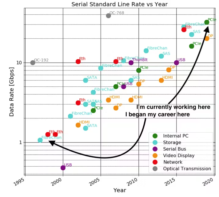
Figure 1: The transformation of SerDes over the last 20 years
SerDes has a background of communication over fiber and coaxial links. The reason is obvious, because sending bytes serially instead of in parallel limits the number of cables! For one or several cables, maximizing the throughput of the cable was paramount. serDes area and power were secondary considerations.
In the mid-1980s, data rates over serial links were largely driven by telecommunications requirements (SONET). During this period, the requirements for OC-1 and OC-3 were not high by today's standards (51.84 Mb/s, 155.52 Mb/s). OC-24 required line rates above 1 Gb/s (1244.16 Mb/s), which was supported by state-of-the-art circuits in bipolar and GaAs processes around 1990.
By the late 1990s, coinciding with an important moment in SerDes history: the OC-24 (2488.32 Mb/s) became available, and OC-192 was planned to be used at about 10 Gb/s. A few years later (early 2000s), 10 Gb Ethernet over 10 Gb/s line rate became a reality (as opposed to XAUI, where four channels were used for 10 Gb/s aggregation).
Another important development began - SerDes was increasingly used for chip-to-chip communication on PCBs and backplanes, replacing parallel links. This development will transform SerDes from an important long-distance communication circuit into a key SoC component. Perhaps the most important example is PCIe, which was introduced around 2002 at 2.5 Gbps and became popular in the mid-2000s.
Various serial data standards were introduced and the status of SerDes research is shown in Figure 1. They include:
Optical transport: OC-192, OC-768, SONET
PC internal: PCIe 1-5
Storage: Fibre Channel, SATA, SAS
Serial bus: USB, Thunderbolt
Video display: DisplayPort, HDMI
Network: SGMII, 1-Gb Ethernet, 10-Gb Ethernet, 25/100-Gb Ethernet
As expected, line rates have been increasing at an exponential rate. The same effect can be seen across categories, with optical transport ahead of the others. The graph includes only the NRZ (PAM2) standard. the PAM4 standard is emerging at line rates of approximately 50 Gb/s.
To understand the circuit-level innovations supporting SerDes development, I used IEEE's Xplore Digital Library to query the International Solid-State Circuits Conference (ISSCC) publications through 2020 to generate a list of ISSCC publications covering "Clocking and Data Recovery" and "SerDes The list of ISSCC publications covering "Clock and Data Recovery" and "SerDes" was generated. The data set was then broken down into
Process type: CMOS vs. non-CMOS (bipolar, biCMOS, HBT, etc.)
Process size: 65 nm, 4 0 nm, 7 nm, etc.
Signaling: PAM2, PAM4
Institutional publication: industrial, academic
Using this dataset, line rates are plotted according to the year of publication (Figure 2). It is estimated that the design of these circuits is approximately one year ahead of publication. However, industrial applications of these publications may lag behind the publication by several years.
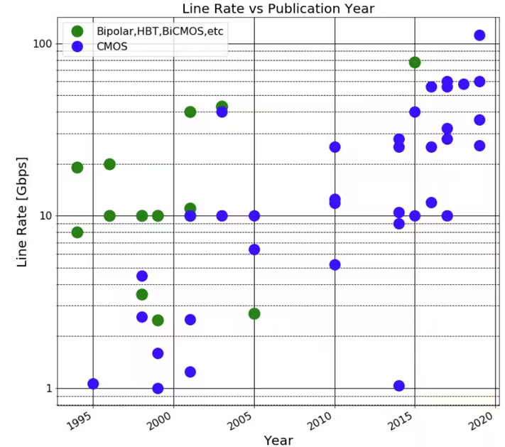
Figure 2: Line rates are plotted according to year of publication
This figure shows that bipolar, biCMOS, and HBT technologies were widely published prior to 2005, but rarely published after 2005. These pre-2005 publications describe the technologies driving optical networking applications where line rate and power/shape factor/integration are secondary considerations.
For much higher capacity SerDes applications such as PCs, storage, video display and networking, it is not just line rate that is critical. The important factors become cost, power consumption, form factor, and integration with large digital cores.
The graphs in Figure 3 are arranged by counting ISSCC data on NRZ/PAM2 versus PAM4 signals. One thing to note is that publications above the 28 Gb/s line rate tend toward PAM4, while publications below 28 Gb/s have almost no PAM4. This fits well with the expected future direction of serial data standards.
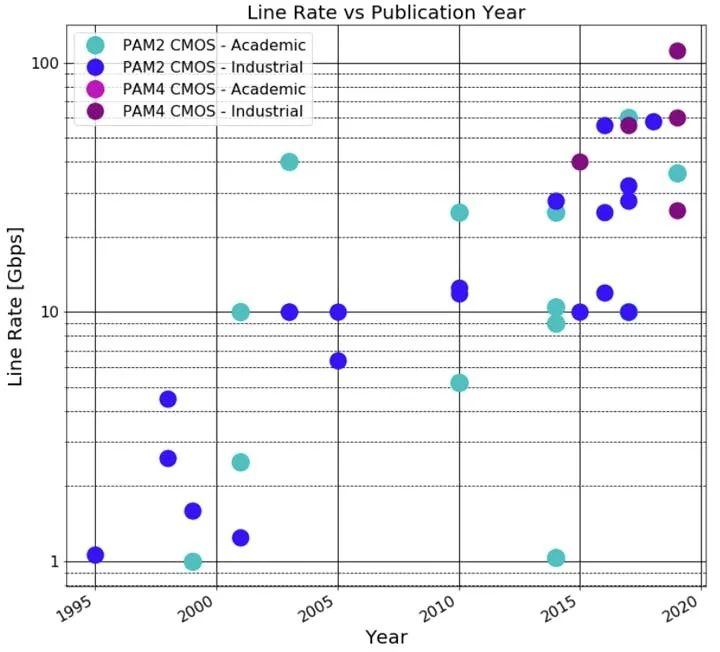
Figure 3: This figure was generated from ISSCC data and covers NRZ/PAM2 vs. PAM4 signaling, etc.
Figure 4 shows the line rate versus the CMOS process size used. The correlation between CMOS process size and line rate can be seen. For example, below 90 nm, most publications are larger than 10 Gb/s. In addition, PAM4 systems are not commonly developed or released above 28 nm due to the need for high integration (ADC, DSP) beyond NRZ/PAM2 SerDes and the high bandwidth requirements of CMOS technology.
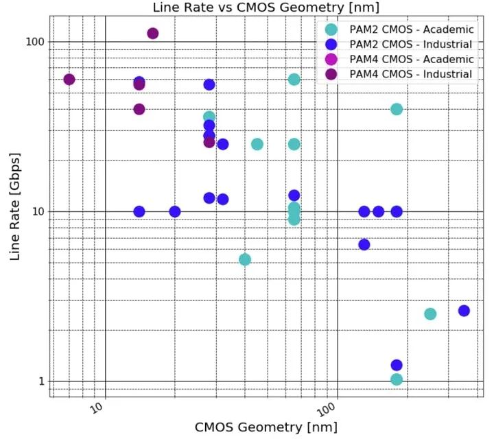
Figure 4: Line ratio versus CMOS size
There is a notable lack of PAM4 related articles in the publications of these academic institutions. This is partly attributed to the search criteria we used. We must emphasize, however, that there are papers related to PAM4 components, but few academics have completed complete PAM4 transceivers. One possible explanation for this is that the PAM4 system (ADC, DAC, DSP, PLL, CDR, etc.) is very complex. Another possible explanation is the cost and acquisition cost of advanced CMOS process sizes such as 7 nm and 14/16 nm.
Combining the data sets from the serial link publication and the serial data rate standard yields the graphs in Figure 5. As can be seen, ISSCC's advanced CMOS circuit design publications are years ahead of the curve in terms of high-capacity serial data standards from network to display. the PAM2 CMOS study made possible PCIe1 to PCIe5 (32 Gb/s), 28-Gb/s Ethernet line rates, etc.
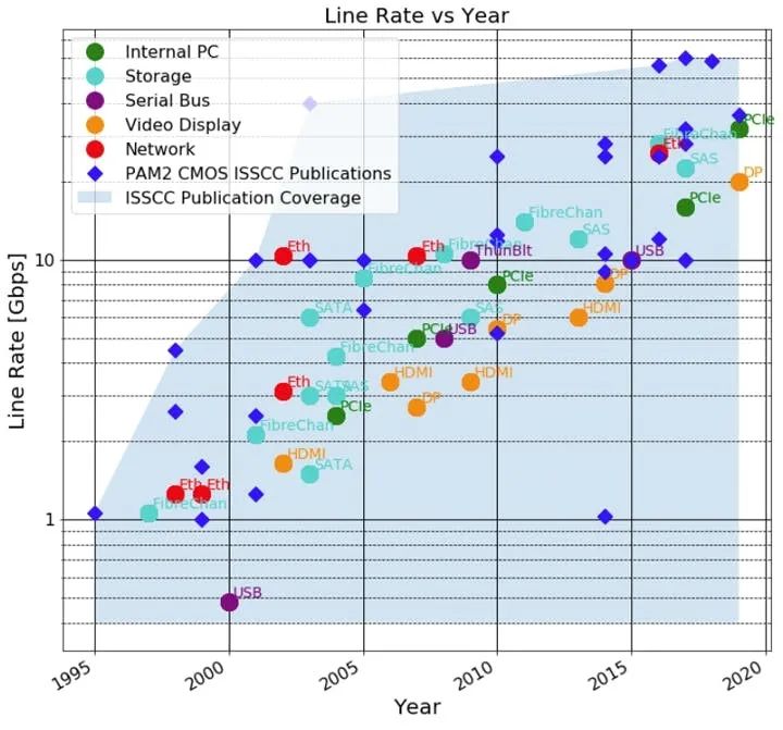
Figure 5, image created by combining data sets from serial link publications and serial data rate standards
First. Pin count and channel advantages
The most obvious advantage of SerDes is the reduced pin count and cable/channel count. For early SerDes, this meant that bytes of data could be sent over coaxial cable or optical fiber.
For modern SerDes, another advantage is the ability to send data bytes over a pair of differential signal pins instead of 8, 16, 32 or N data pins and a clock pin. This aspect of serialization can be cost saving due to smaller packages and denser PCBs. The specific advantages depend on die cost, package cost, PCB cost, PCB congestion and other factors.
Second, the distance advantage
Over the last decade, SerDes' ability to transmit over long distances across PCBs and backplanes has helped them enter many new areas.
From basic microwave designs, we know that when the flight time is less than the rise/fall time, the transmission line looks like a "lumped element. For parallel interfaces with GPIOs, the rise/fall time is typically no less than a few nanoseconds. This sets the distance a parallel unterminated interface can operate on a typical PCB to about 30 cm. Terminating the parallel bus increases the coverage; however, at the same time, it adds a lot of power and dramatically decreases power efficiency (Figure 6).
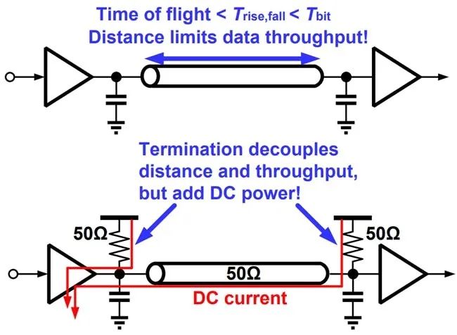
Figure 6: While terminating the parallel bus increases coverage, power efficiency drops dramatically
The SerDes interface is typically transmitted over a controlled impedance transmission line terminated at both ends (TX, RX). This allows bits to be transferred quickly without worrying about reflections. Of course, there is a lot of additional complexity involved in trying serial transmission quickly - such as serializer, deserializer, TX PLL, RX CDR, feed-forward equalization, receive equalization, etc.
Third, the power consumption advantage
Until recently, SerDes had the power advantage over serial data buses. The ideal parallel bus consumes power to charge and discharge the TX and RX capacitors as well as the trace capacitance. Trace capacitance can be important on FR4 when considering distances of 10, 20 or 100 cm.
According to the first principles, we know that the power of the LVCMOS link is ~C*V^2*f. In the case of data, the frequency is the total bit rate multiplied by one half of the conversion density. The total number of conversions and the power are independent of the number of channels required for first order - the more channels, the fewer conversions per channel. For a 1-Gb/s link, 10 cm to 1 m may require 8-16 channels. For a 10-Gb/s link, 1 m may require a very impractical 120 channels!
Figure 7 shows the power of parallel LVCMOS links at different voltages versus the power consumed by SerDes from the 1990s to today. As can be seen, modern SerDes have the power advantage over longer distances, but the power advantage is not yet clear.
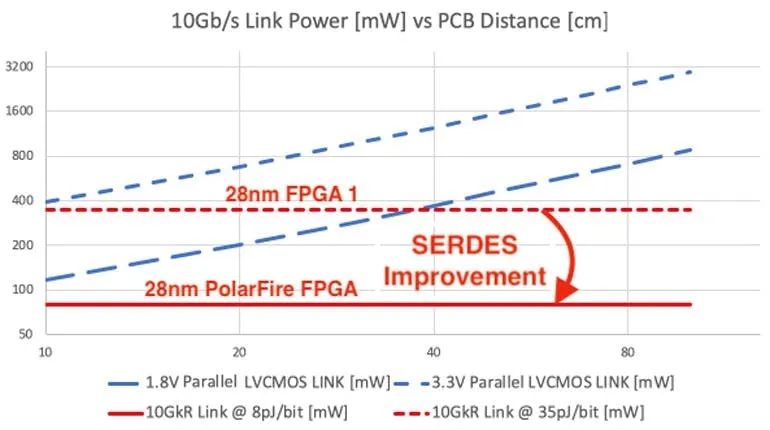
Figure 7, comparing the power of parallel LVCMOS links with different voltages to the power consumed by SerDes in the 1990s and today
Where SerDes really shines in terms of power is at higher data rates. Figure 8 shows the power of parallel LVCMOS links at different voltages versus the power consumed by various production 28nm SerDes in the mid to late 2010s. It can be seen that modern SerDes maintain a power advantage at almost all distances. For the power-optimized SerDes, the power advantage is very clear at all distances.
Picture
Figure 8, Power of parallel LVCMOS links at different voltages compared to power consumption of various 28nm SerDes in the mid to late 2010s
As process technology advances, the power advantage of SerDes will of course continue to grow.
As discussed in the previous section, SerDes offers compelling advantages in power consumption, pin count, and range. the downside of SerDes is the complexity and cost associated with SerDes.
I. Complexity
At a minimum, for low data rates, a good TX PLL, RX CDR, TX driver, and RX front end are required. Each of these is a complex analog subsystem. Designing these blocks and the entire SerDes system requires a team of skilled analog/mixed-signal designers to accomplish. These blocks (along with the complex digital controls) include:
1. Good TX PLL: This block is needed to generate typical multi-gigahertz clocks from a typical 25 to 100 MHz reference clock with very low (~1 ps or better) long-term jitter.
2. Good RX CDR: This block is a complex control loop for tracking the average phase of the input data despite any noise, distortion or crosstalk on the link. This is usually done using a complex phase rotator or CDR driven PLL.
3, TX line driver: This module converts serialized data into a typical 50 Ω differential signal, usually with precursor and post-cursor emphasis.
4. RX Equalizer: This block attempts to equalize high-speed channel effects using either a continuous-time equalizer or DFE or both. An automatic gain control (AGC) circuit is usually required to facilitate equalization. the RX equalizer usually includes an automatic calibration routine as state machine logic or software.
5. High-speed serializer and deserializer logic
All of the modules listed above require significant design time by experienced design teams (. As data rates increase (Gb/s) and efficiency requirements increase (pJ/bit), this increases the complexity and cost of the SerDes. As reliability requirements increase, more and more aging and electromigration simulations must be run and analyzed, further driving up costs.
Fortunately, SerDes is already widely used as an IP block. As a result, system companies can license validated designs from leading IP design providers. In this way, complexity is handled by dedicated design teams and development costs can be shared across multiple chips, projects and even industries, helping to reduce costs.
II. Costs
The primary costs of SerDes come from design (many chip designers spend many years) and verification, but secondary considerations such as chip area and PCB area are also important.
SerDes verification at the PMA level is typically handled by the design team or a subset of the design team. At the system level, verification can be very complex, especially for standards such as PCIe.
For complex serial standards, a testbed (typical in System Verilog) is required to verify the system from the physical layer (including PMA and PCS), the data link layer, the transaction layer, and the device level. Verification covering these levels typically examines protocols, patterns, negotiation, error injection and recovery, etc. Verification also typically requires many person-months and often involves third-party verification IP (VIP).
On die, SerDes may be cheaper or more expensive than parallel interfaces. Depending on the process node, SerDes may consume about 0.15 to 0.5 mm 2 per channel. parallel interfaces can be much smaller than this, but require more I/O. Therefore, depending on whether the chip is I/O-constrained or pin-constrained, SerDes may result in more or less die cost than parallel interfaces.
At the package and PCB level, SerDes allow for a reduced number of pins and alignments. As a result, they should lead to smaller, lower-cost package and PCB designs. However, due to the complexity of high-speed controlled impedance (e.g., 50 Ω) traces, packages and PCBs using SerDes can be more difficult to design and therefore more expensive than PCBs using slower parallel interfaces.
We have seen incredible growth rates in the interface IP category over the past 20 years, and we expect the category to generate a consistently high source of IP revenue for at least the next 10 years. But if we look deeper into the various successful protocols such as PCI Express, Ethernet or USB, we can find a common function in the physical (PHY) part, the serializer/deserializer (SerDes) function.
In 1998, advanced interconnects used in telecom applications were based on 622 MHz LVDS I/O. Telecom chip makers were building huge chips integrating 256 LVDS I/Os running at 622 MHz to support network architectures. Today, advanced PAM4 SerDes operate at 112 Gbps; supporting 100G Ethernet over a single connection. In two decades, SerDes technology has jumped 180 times in efficiency!
If we make a quick comparison with CPU technology. in 1998 Intel released the Pentium II Dixon processor at 300 MHz. in 2018, the Intel Core i3 runs at 4 GHz. In 20 years, CPU frequencies have increased 15 times. Most comparably, as mentioned above, SerDes speeds have increased 180 times.
SerDes are now used not only for telecom, but also for more applications connecting chips and systems. in the late 2000s, smartphones integrated USB3, SATA and HDMI interfaces, while telecom and PCs/servers integrated PCIe and Ethernet. These trends led to the interface IP market becoming a massive IP category, growing by more than $200 million at the time. It is small compared to the CPU category, which is four or five times larger. However, since 2010, the interface category has grown at least 15% year-over-year. It is the fastest growing category compared to all other semiconductor IP categories (e.g., CPUs, GPUs, DSPs, libraries, etc.). The reason is directly related to the growing number of connected devices each year, each exchanging more data (more movies, pictures, etc.), and connectivity is the beginning of the communication chain.
During the decade of 2010, the global community was almost completely connected. With connection rates and the number of data centers increasing rapidly over the last decade, Ethernet became the backbone of that connectivity. If we use SerDes rates as a metric, it was 10 Gbps in 2010, 28 Gbps in 2013, 56 Gbps in 2016 (allowing for 10G, 25G and 50G Ethernet support respectively) and 112 Gbps in 2019.
Then, in 2017, emerging data-intensive computing applications such as machine learning and neural networks began to see an explosion in demand for high-speed connectivity, increasing the growing need for high-bandwidth connections. At the same time, analog mixed-signal architectures, which have been the standard for SerDes designs from the beginning due to the evolution of CMOS technology to advanced FinFETs, became extremely difficult to manage and more sensitive to process, voltage, and temperature variations. In modern FinFET nanotechnology, building transistors involves stacking individual electrons given the tiny size of the transistors. As a result, it is extremely difficult to build precision analog circuits that can withstand changes in stressful environments.
But the positive aspect of advanced technologies such as 7nm is that you can integrate a staggering number of transistors by the square millimeter (densities of 100 million transistors per square millimeter), so new digital-based architectures (DSPs) can now be developed using digital signal processing to do the vast majority of the work in the physical layer. DSP-based architectures support the use of higher-order pulse-amplitude modulation (PAM) modulation schemes than the non-return-to-zero (NRZ or PAM2) used in past analog mixed-signal approaches.PAM 4 doubles the data throughput of the channel without increasing the bandwidth of the channel itself.
For example, a channel with a 28 GHz bandwidth can support data throughput of up to 56 Gbps using NRZ signaling. By using PAM-4 DSP technology, this same 28 GHz bandwidth channel can now support 112 Gbps data rates! When you consider that the analog SerDes architecture is limited to a maximum of 56 Gbps for physical reasons (possibly less ......) .PAM-6 or PAM-8) for physical reasons.
Using a DSP-based SerDes is not only necessary to build a robust interface in FinFET technology, but it is also the only way to double the data rate to more than 56 Gbps, for example. 112 Gbps with PAM-4 and 200 Gbps with PAM-8.
As the market evolves, Chiplet seems to be surging, and starting later this year, most advanced SoCs will also be 3nm designs. This will make integration of high-end IP like SerDes too risky, leading to externalization of this functionality into Chiplets designed in more mature nodes like 7 or 5nm. If interface IP vendors are going to be major players in this revolution, then silicon foundries that address the most advanced nodes and build major SoCs like TSMC and Samsung will play a key role.
We don't think they will design small chips, but they could decide to support IP vendors and push them to design small chips for use with 3nm SoCs, just as they are doing today in supporting advanced IP vendors to market their high-end SerDes as 7nm and 5nm hard IP.
There is no doubt that SerDes has many opportunities ahead.