Date:2023-04-03 10:51:22 Views:1118

Diamond semiconductors are known as the "ultimate power semiconductors" because of their superior characteristics to other semiconductor materials. Based on the industry's long-term research and development activities, diamond semiconductors have now begun to gradually move toward practical use. However, it will still take a long time for the application of diamond semiconductors to become popular, but it has been reported that the prototype of diamond semiconductors will appear in a few years at the earliest. The more attention the industry pays to diamond semiconductors, the easier it is to gather superior resources and accelerate the speed of research and development.

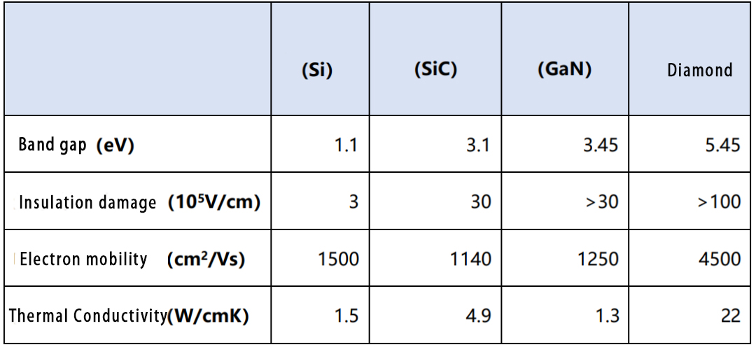
I have written about diamond semiconductors in the past, so let's review their characteristics again. As shown in the table below, diamond is far superior to other semiconductor materials in terms of band gap, electron mobility, and thermal conductivity. Compared with silicon carbide (SiC) and gallium nitride (GaN), which are already commercially available, diamond has excellent characteristics and is therefore known as the "ultimate semiconductor material". Diamond is also expected to be used in the space field, where semiconductors are not yet widely used, because of its high radiation resistance. In addition, diamond can be used not only in semiconductors but also in quantum sensors. With the promotion of quantum computer R&D activities, more and more universities and R&D institutions are advancing the development of diamond.
It is mainly Japanese R&D institutions that are leading the R&D work on diamond semiconductors. Between 1980 and 2000, the Japan Institute for Inorganic Materials Research (now NIMS) and the National Institute of Advanced Industrial Science and Technology (hereinafter referred to as "AIST") produced many achievements, such as the crystalline synthesis method, the production of p-type semiconductors, n-type semiconductors, etc. In particular, NISTRI's research and development is second to none, even today, with its full range of research and development, such as the growth of diamond crystals, the manufacture of wafers, and the development of components such as diodes and transistors. However, the R&D activities to date have been limited to validation work in the laboratory, and no actual semiconductors have been developed that can be used in electronic circuits and devices.

The above table was created by me based on the information from Sogo Research.
(Table from: eDevice Industry News)

One of the main reasons why the development of diamond semiconductors has been limited is that the diameter size of diamond wafers is too small to meet the demand. (Toyonaka City, Osaka, Japan; hereinafter referred to as: "EDP"), a subsidiary of Sankei Research, has been on a mission to expand wafer size since its founding in 2009, and has long been quietly working in the semiconductor industry, developing new technologies to promote corporate growth.
The upturn in business conditions stems from the rise of the gemstone (diamond) market. Diamonds as jewelry are generally popular with natural diamonds, while man-made diamonds are less valuable. During the period from 2015 to 2019, large diamond manufacturers assigned high values to artificial diamonds, which led to a rapid expansion of the market for artificial diamonds in the jewelry category. The demand for EDP's monocrystalline diamonds as a crystal type has increased dramatically, acting as a "catalyst" for the company's growth. As a result, EDP went public in 2022 and gained a resource base to ensure the development of semiconductor wafers.
EDP's recent performance has been sluggish due to the global economic situation that directly affects the diamond market used as an accessory. However, in the medium to long term, the trend of converting natural diamonds to artificial diamonds will not change, taking into account factors such as environmental protection issues and protection of workers' rights in developing countries, and EDP's position as a supporting company for diamond in the direction of semiconductors will become increasingly important.
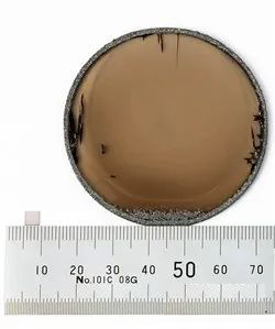
In addition, Orbray Corporation (head office: Adachi-ku, Tokyo, Japan; name changed to "Orbray" in January 2023; Chinese name: Orbray Co. material wafer business. "Orbray has developed a method for producing diamond wafers with heteroepitaxial growth using sapphire as a substrate, and has already succeeded in producing wafers with a diameter of 2 inches. The goal is to produce 4-inch and 6-inch wafers in the future. In addition to semiconductor applications, Orbray is also developing ultra-high purity wafers for quantum computers using other growth methods, with the goal of commercialization.

"A 2-inch diamond wafer developed by Orbray.
(Image from: eDevice Industry News)
Semiconductor wafer R&D and capacity expansion are currently in the development stage, and "it is easier to obtain wafers for R&D than in the past" (Diamond Semiconductor R&D Technician). Nowadays, if a researcher is interested in R&D wafers, he or she can easily obtain them in kind, which is a significant improvement compared to the past.

Today, more and more organizations are moving diamond semiconductors from the R&D stage to practical use. Professor Makoto Kagami of Saga University in Japan has been developing diamond semiconductors for more than 20 years. About five years ago, Prof. Kagami learned about Orbray's diamond wafers and realized that they could be used for research and development, and the two companies began joint research and development. semiconductor. The result is a diamond semiconductor with the highest performance in the world, and it is second only to the one achieved by the Massachusetts Institute of Technology (MIT) using gallium nitride (GaN) in terms of semiconductor performance. (GaN).
He believes that it is necessary to move the verification of semiconductors from the R&D stage to the practical stage, and has set the goal of developing diamond transistors within five years. He is also working with companies involved in packaging, bonding, and other peripheral technologies to promote research and development, and is measuring the lifetime of transistors to verify their long-term reliability. In addition, Prof. Seiji Kaji is planning to test power electronic circuits to verify their operation.
In addition, Nidec is making effective use of its long experience in "one-stop" technology (from crystal growth, wafer processing, to chip fabrication) to promote the practicalization of chips. The goal is to achieve the performance (e.g., current and voltage values) required by existing chips using large-area chips (chips). The policy is to work on both wafers and chips at the same time.
In August 2022, Power Diamond Systems ("PDS"), a subsidiary of Waseda University, was established as a start-up company with the business goal of "making diamond semiconductors practical. The company's goal is to bring the research and development of Professor Yo Kawaharada, a pioneer in the diamond semiconductor industry, to practical use.
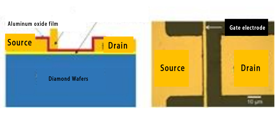
Professor Kawaharada is known for his development of diamond field effect transistors (FETs) using the basic technology of diamond semiconductors (hydrogen termination surfaces). PDS plans to collaborate with many companies (such as wafer fabricators, power semiconductor manufacturers, electrical equipment manufacturers, etc.), universities, and R&D institutions in order to make diamond semiconductors practical. PDS aims to build a complete ecosystem from materials, chips, and systems to achieve its goal of becoming a "leading player" in the industry.

The world's highest-performance diamond semiconductor developed by Professor Makoto Kaji.
(Image from: eDevice Industry News)
Although PDS has been established for more than half a year, it has already established good relationships with many major companies and R&D institutions in Japan. And we plan to release trial works in a few years, and then develop systems related to power electronic circuits in one year one by two years.

Mr. Tatsuya Fujishima, CEO of PDS, said, "There are many companies in Japan that have a lot of experience in producing power semiconductors and high-frequency components," with regard to the practicality and potential of diamond semiconductors. The next task is whether to start cooperation with large companies. Unfortunately, however, it seems that companies have not been very active in the R&D process in the past. A researcher said, "At the launch of R&D results such as the Institute, engineers from companies showed great interest, but none of this was directly related to business." It will take at least another decade or so to actually commercialize, and the R&D results will not bring profits directly and quickly, which is why companies have been hesitant to do so. However, universities and R&D institutions alone cannot achieve real social-side applications.
In addition, the speed of overseas enterprises outside the R & D really surprised the author. In the author's interview had found that in response to the R&D projects of Japanese R&D personnel, the R&D personnel of enterprises in Taiwan and mainland China have made applications for collaborative R&D. In the face of the current severe risk of landscaping, Japanese R&D personnel should be cautious about cooperating with overseas. However, as Japanese companies are not willing to pay attention, it is inevitable to advance R&D with the help of overseas companies.
Compared with silicon carbide (SiC), gallium nitride (GaN) and other semiconductors that have already been made practical, diamond semiconductors do not have a high enough level of interest at the social and national levels. Since several organizations in Japan have already started to take a critical step toward the practical realization of diamond semiconductors, it is important for the government and companies to take action as soon as possible.