Date:2022-12-27 10:40:55 Views:949
The ability of light to propagate high data rates with relatively low power consumption makes it an excellent information carrier. Silicon has been the cornerstone of semiconductor technology for decades. It was only a matter of time before the two were brought together: a technology that harnesses the power of light, using the same platform that pushed microelectronics to its peak. After all, why reinvent the wheel when billions of dollars have been invested in perfecting the materials and processes used to make microelectronics?
And so silicon photonics was born. First explored in the 1980s and beginning to gain momentum at the turn of the century, the technology has been commercialized in volume up to now. It has proven increasingly popular in data centers, where silicon photonics-based transceivers support optical connectivity between servers.
The technology is expected to grow rapidly over the next decade as the world's appetite for data grows by the day and the desire to reduce energy consumption. Market research firm Yole Group expects the silicon photonics market to grow at a compound annual growth rate (CAGR) of 36 percent from 2021 to 2027, when it will reach nearly $1 billion.

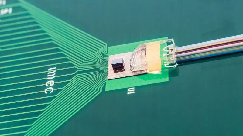
Hybrid CMOS-silicon photonic transceiver prototype developed by Imec
While the primary driver of this growth is communications within data centers, emerging applications are expected to emerge. Silicon may be used for data exchange over increasingly shorter distances, and eventually between chips in the same system. The technology is also operating as a base platform for automotive lidar, allowing self-driving cars to drive on the road, or at least help drivers avoid collisions.
"Silicon Photon is manufactured in a 300mm standard semiconductor fab. This means it can be produced with tight specifications and quality control as well as reliable logistics. This offsets some of its limitations and makes it an attractive benchmark for combining with other technologies such as lasers," explained Carol de Vries, Photondelta's chief technology officer. He added that preliminary market forecasts indicate that silicon photonics, either alone or in combination with other integrated photonics platforms, is here to stay. "It is expected to have a 45 percent market share by 2040."
Traditionally, silicon photonics (SiPh) has been understood as integrated photonics based on materials that dominate conventional electronic circuits: silicon and silicon oxide (silica). In the scientific literature, this type of integrated photonics is often referred to as silicon on insulator (SOI), a term also used for specialty semiconductor technologies.
In this strict sense, SOI is probably the most limited technology in the three-member integrated photonics family, which also includes technologies based on silicon nitride (SiN) and indium phosphide (InP). Because of its indirect bandgap, silicon cannot produce gain or laser light, meaning the material cannot be used to build active components such as light sources and amplifiers. the same is true for SiN, but this material has lower light loss and wider spectral coverage than SOI.
InP is the only semiconductor that can perform all functions without external help, but also has the disadvantages of SOI in terms of loss and spectral coverage. Both Si and SiN platforms typically rely on some form of integration with InP if used only as a light source. The best approach is application-specific.
Of course, the properties of SOI are sufficient for many interesting applications. Light can move efficiently in and out of the chip, and important passive components such as gigahertz modulators and photodetectors can be used. In addition to this, decades of silicon processing experience can be leveraged - 300 mm wafers, high yields, co-integration with CMOS, various advanced 3D integration techniques - and there is plenty of room for silicon photonics.
Increasingly, however, SiPh is being interpreted as any type of integrated photon that can be fabricated in a CMOS fab. In that case, SiPh and SiN become a single entity, since the latter is also compatible with CMOS. But there's a caveat, explains Imec silicon photonics researcher Joris Van Campenhout. "Manufacturing high-end SiN waveguides with very low light loss requires a high thermal budget. This may be incompatible with co-integrating other functions."
Maintaining CMOS compatibility is often limited, Van Campenhout notes, "The CMOS manufacturing environment is tightly controlled. Certain materials are prohibited, including InP and other Group III-V semiconductors." On the other hand, the precepts of CMOS are not set in stone. Over the past few decades, fabs have introduced several new materials to keep Moore's Law in operation. "If you have a strong business case, anything is possible. However, no integrated photonics application has yet been able to generate the volume that would guarantee such adjustments in a mainstream fab."
However, Van Campenhout notes that future use cases will require SiPh to introduce new materials to continually improve performance and cost. For example, as signal rates in data center transceivers exceed 200 Gb/s, achieving sufficient modulator bandwidth and acceptable optical loss becomes challenging. These obstacles can only be removed by introducing new materials into the mix. "Enriching SiPh with new materials and features while maintaining maximum CMOS compatibility is a great opportunity."
New materials can be introduced while adhering to CMOS rules by integrating "disabling" materials or components containing them outside the front-end processing environment (i.e., the back-end production line). "Today, it is unclear what the most appropriate level of integration is and when it will occur at scale. Beyond data and telecommunications, applications research is still in its infancy. What functions do you need to integrate? What specifications are needed? For a wide range of applications, these are questions we still can't answer. That said, I think it's fair to say that as SiPh gains traction, the business model solidifies and market pull increases, the boundaries will prove not to be as difficult as previously thought."

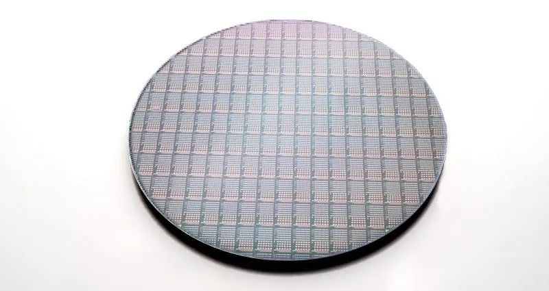
A 300 mm silicon photonic wafer with a flip-flop InP laser diode
Historically, optical communication links have become shorter and shorter, from connecting continents to homes and offices to servers within data centers. They will get shorter, in the 1-10 cm range, as the electrical connections between chips begin to lose power.
Currently, this problem is most pressing at the high end of high-performance computing applications. For example, Nvidia's "all-in-one data center" combines eight powerful GPUs and a lot of memory to handle demanding machine learning and data science workloads. The system's performance depends on how quickly and efficiently the processors and memory can exchange data, and Van Campenhout estimates that they will become a bottleneck after two or three generations, based on current electrical interconnect speeds.
Van Campenhout has been the director of Imec's optical I/O R&D program since 2014. For the past decade, his research focus has tended to be on data communications and telecom applications, but recently, industry interest in short-haul optical interconnects has increased dramatically, he said. "Many companies, including several well-capitalized startups, are looking to aggressively deploy deeply integrated short-haul optical interconnects to improve the performance of their high-performance computing systems."
In addition to its optical I/O R&D program and SiPh/SiN prototyping services at its Leuven headquarters, Imec has launched a series of application-oriented silicon photonics activities in the Netherlands. Co-funded by the National Growth Fund and in collaboration with TNO and other partners in the Photondelta ecosystem, the collaboration will focus on lidar and laser design at the Holst Center in Eindhoven and agri-food applications at Oneplanet in Wageningen.
"It is fantastic to see the investment of the Dutch Ministry of Economy with the National Growth Fund Photondelta. This financial impulse is crucial, as the industry is in an investment phase globally. In addition, these funding mechanisms facilitate collaboration.
Photondelta provides an excellent opportunity to strengthen collaboration within the Holst Center with local partners and across borders," commented Kathleen Philips, Vice President of Research and Development at Imec and General Manager of Imec at the Holst Center.
"At Imec NL, we are focused on designing more complete photonic systems, including electronics and algorithms. Application areas are agri-food and health, as well as data communications and automotive LIDAR. In addition, the new system design activity at the Holst Center bridges the gap between our long-term photonic technology activities in Belgium and our research on photonic applications at Oneplanet in Gelderland."
In the future, this technology may penetrate into more general applications. For example, leading chip manufacturers are focusing on "partitioning" their chips into multiple ICs, each with specialized functions (CPU, I/O, cache, etc.). Especially in this case relatively long distances, copper wire may not be able to handle the interconnection of these small chips.
This will require further improvements in bandwidth and power efficiency. In Imec's roadmap, the goal is to double the bandwidth of the optical subsystem and halve the power per bit every two years. As Van Campenhout has explained, this will require the introduction of new materials that could "break" CMOS compatibility. But if there is a business case for meeting this challenge, it is likely to be inter-chip optical interconnects. "It's going to be an exciting journey," Van Campenhout said.