Date:2022-12-21 11:43:00 Views:769
1 Celebrating the 75th Anniversary of the Transistor
In 1947, the invention of the point-contact bipolar transistor provided the world with a powerful switch to control current and enhance the cost effectiveness of electronics. The foundation of the digital age was the invention of the integrated circuit, which enabled the miniaturization of transistors and other circuit components.
In 1965, Gordon Moore observed and described a trend in the semiconductor industry where the number of transistors that could fit on an integrated circuit doubled every year. in 1975, this rate was revised to double every two years. "Moore's Law" provides the basis for understanding how ICs are revolutionizing the digital world.
The semiconductor industry's dedication to Moore's Law has made the transistor a key enabling technology decades after its invention. This is largely because engineers and scientists see opportunities for innovation where there are significant challenges. The fact that challenges and opportunities for innovation are essentially two sides of the same coin has become part of the fabric of the semiconductor industry.
In addition, the semiconductor industry has never allowed itself to be overwhelmed by the tremendous pace of Moore's Law. It has always excelled at identifying near-term and long-term bottlenecks for integrating more functionality and making the innovations needed to address them. Through research, this iterative process of conquering the next mountaintop is feasible and worthwhile. This incremental approach has been the cornerstone principle behind the continued cadence of Moore's Law.
2 The Evolution of Moore's Law's Focus Area
The benefits of technology scaling for products have persisted for decades through revolutionary and incremental innovations. These innovations remove the bottleneck of integrating more powerful features.
Dennard's Law of Scaling: In 1974, Robert Dennard and others authored a seminal paper describing a transistor scaling rule that enabled simultaneous performance improvements, power reductions and sustained density gains.The principles in Dennard's work were adopted by the semiconductor industry as an effective roadmap to drive Moore's Law for the next 30 years, providing a predictable path for continued improvement in transistor technology. Key examples of bottleneck breakthroughs are (a) innovative immersion lithography to pattern features below the wavelength of light for continued density scaling, (b) innovative processes and tools for atomic-level precision engineering of ultra-thin gate oxides and ultra-shallow junctions to address electrostatic control bottlenecks below 30nm gate length, and (c) transition of wafer size from 100mm to 300mm to increase fab yields and reduce costs.
Post-Dennard Scaling Law: While Dennard's scaling law helped realize the substantial benefits of Moore's law, it did not incorporate transistor subthresholding and gate leakage into its power consumption model. By the mid-1920s, the continued reduction in transistor threshold voltage and gate oxide thickness, which supported voltage scaling to reduce power, began to cause leakage currents to exceed transistor switching energy. In addition, simple size scaling of interconnects led to resistivity bottlenecks, which could limit circuit performance. Breaking this bottleneck will require the expansion of additional innovation focus areas, primarily three different paths that will continue to coexist in the future to achieve continued performance improvements and power reductions.
Innovation Path 1: Lithography, Materials and Device Architecture: Improving the resolution of lithography exposure tools has been a fundamental driver of scaling since the beginning of the semiconductor industry. Introducing high NA EUV to HVM can significantly improve lithography resolution. High NA EUV lithography is the most complex machine in the world, and new materials and device innovations mention break through bottlenecks that limit computational performance and cost. Some typical examples include (a) transistors: strained Si (mobility gain), high-k/metal gates (gate leakage reduction), FinFETs (improved electrostatic techniques for continuous voltage scaling), and (b) interconnects: low resistance Cu (instead of Al) using chemical mechanical polishing to support denser and multilayer interconnect circuits, and continuous scaling for routing power and delay of Low-k.
Innovation Path 2: Design Technology Co-optimization: Building on the first path, over time, design and technology experts worked together to identify opportunities to go beyond size scaling or pure material/device innovation advantages through DTCO, while addressing other subsequent technical bottlenecks. Advances in electronic design automation (EDA) capabilities unleashed rapid design prototyping, which is used today to explore a wide range of technology features. DTCO brought innovations such as contact on active gate (COAG) to reduce the height of logic bank cells, fin trench isolation (FTI) to reduce spacing between digital logic cells, and cell height reduction in logic banks through fin depopulation. The combined optimization of interconnect stack design, EDA placement and routing, and layer filling algorithms continue to significantly improve performance at each technology node. DTCO is an important part of maintaining technology scale today.
For example, to continue scaling cell heights, we need to develop more complex interconnect solutions. PowerVia technology (Figure 1), which moves the power lines to the back of the wafer, enables more cell height and performance scaling than simple geometric shrinkage. Another example is the next major architecture for transistor scaling, called RibbonFET or Gate All-Around, as shown in Figure 2. With the migration to Ribbon FET, performance scaling is achieved by adding additional nanoribbons. Each additional nanoribbon increases the drive current.
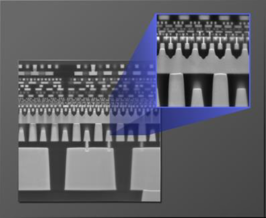
Figure 1. Intel's backside power delivery solution, PowerVia, which separates the power and signal lines and reduces the standard cell size. The power lines are placed under the transistor layer on the back of the wafer.
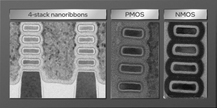
Figure 2. Intel's RibbonFET omni-directional gate (GAA) transistor architecture stacks four nanoribbons to achieve the same drive current as multiple fins, but with a smaller footprint.
Innovation Path 3: System Technology Co-Optimization: Today, the industry faces a new set of challenges and opportunities in optimizing system performance with continuous technology scaling. Providing efficient memory bandwidth and effective power delivery are key challenges in translating technology scaling into system performance. The additional differential scaling of kernel logic (standard cells) and cache (SRAM), and the need for cache/core in HPC architectures, drives the opportunity by separating large caches from the top-level nodes. This will require significant and scalable innovation in wafer stacking to achieve optimal performance and total cost of ownership.
Going forward, semiconductor processing, materials and device architecture innovation, as well as DTCO and STCO, will continue to be important innovation paths for scaling technologies to enable the needs of next-generation accelerated computers.
3 Advantages and Challenges of STCO
In pursuit of Moore's Law greater functional integration of 3D-ICs, the first step for STCO is to optimize the silicon content in the package. 3D-ICs achieve greater functionality by introducing more components into the package. The role of packaging and its contribution to Moore's Law scaling is evolving and offers entirely new ways to optimize systems. Until 2010, the primary role of the package was to transfer power and signals between the motherboard and the silicon, and to protect the silicon. Now, emerging 2D and 3D stacking technologies provide architects and designers with the tools to integrate heterogeneous technologies in compact packages and further increase the number of transistors per device by interconnecting multiple small chips at higher bandwidths and connection densities. Moore predicted that the focus area of functional integration would continue to evolve. His 1965 paper noted that "it may be more economical to build large systems with smaller functions packaged and interconnected separately. And the availability of powerful functions, combined with functional design and construction, should allow large system manufacturers to design and build large numbers of devices quickly and economically." Today, packaging is done at the fab level, using actual wafers. The line between fab and chip packaging has blurred to the point of being indistinguishable.
As more and more functionality is integrated into the package, where the system is essentially folded into the package, the amount of silicon exceeds the amount that can be built within the limits of the photolithography mask. This functionality must be split across multiple silicon components, using advanced packaging techniques to provide low-latency, low-power, high-bandwidth interconnects between multiple chips. Cost optimization of the yield pushes the maximum chip size to a lower level, driving further silicon disaggregation into smaller, smaller chips. Once decomposed, there are options to optimize the design and silicon process characteristics, cost, functionality and IP module availability for each small chip.
STCO is a larger level of functional integration where all individual areas of the system: software (expressed as workloads), system architecture, design engineering, IP building blocks, silicon fabrication consisting of transistors and interconnects (plus associated materials), voltage regulation, advanced packaging for heterogeneous integration, test and high volume manufacturing are all co-optimized to create products that support customer innovation and applications . In essence, we can think of STCO as assembling many of the technologies that once existed across an entire motherboard in a compact package.STCO starts by integrating the full functionality of the system and then jointly optimizing each component.STCO relies on continuous advancements in all areas of the system (hardware and software) while optimizing collaboratively as a whole. Figure 3 is an illustration of the areas covered by STCO for general-purpose computing systems. Most of the historical specifications have been jointly optimized across adjacent layers, such as silicon technology and underlying IP in Figure 4. Figure 4 illustrates the differences in the domains covered between device optimization, DTCO, 3DIC, and STCO.
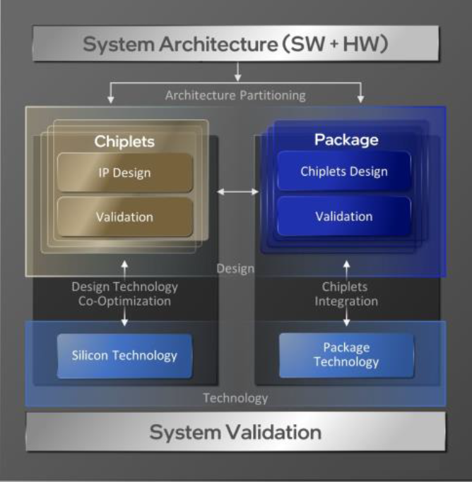
Figure 3. System technology co-optimization for computing systems.
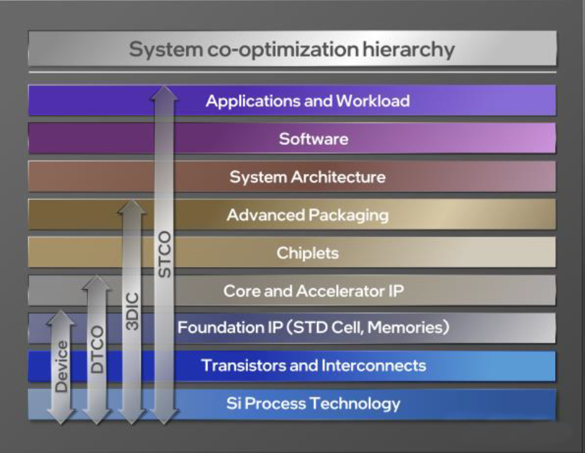
Figure 4. Hierarchy of system technology co-optimization. illustrates the differences between device optimization, DTCO, 3DIC, and STCO.
The motivation for STCO is the same as that which has driven Moore's Law for decades: the quest to eliminate bottlenecks and achieve higher levels of integrated functionality at lower cost. STCO starts with workload analysis and application usage to evaluate and optimize combinations of technology types (e.g., logic, memory, analog, voltage regulation), designs, decompositions, and resynthesis configurations. By optimizing by workload and application type, higher levels of performance and functionality can be achieved.
As mentioned earlier, Moore's Law is about adding greater functionality to the integration. In STCO, each functional bottleneck (e.g., power or performance) can be addressed by providing synergistic optimization in terms of silicon technology, small-chip decomposition, and resynthesis within advanced packages to optimize workloads and applications. This is shown in Figure 5, which demonstrates how bottlenecks are eliminated to unlock new functionality. This is very similar to the silicon scaling that the industry has focused on for years, but now applied to a broader range of capabilities to improve integrated functionality.
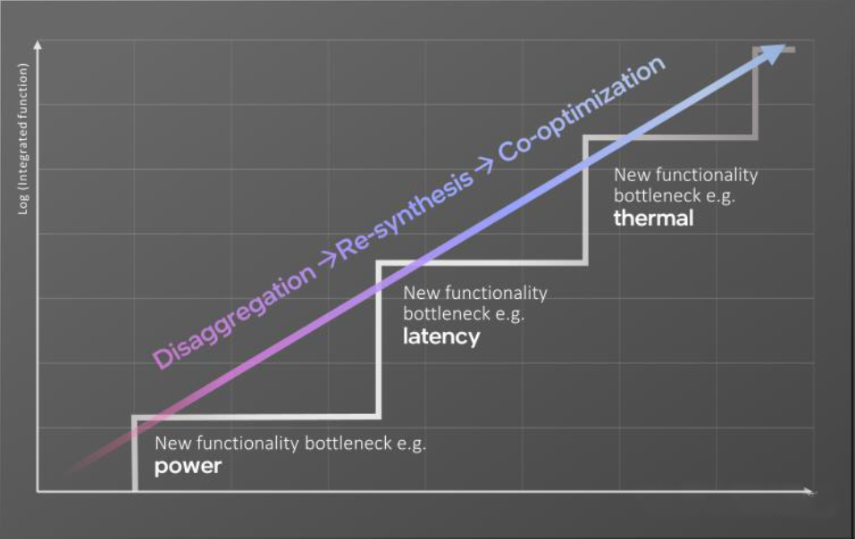
Figure 5. Decomposition, resynthesis and co-optimization used to address Moore's Law bottlenecks.
As a specific example, Figure 6 shows the new system design functionality that is enabled by a chip-to-chip bond pitch scaling roadmap (starting with micro-bumps and then moving to hybrid bonding). As the chip-to-chip bond pitch decreases, higher connection densities (number of connections per mm²) can be achieved. Higher connection densities enable functional decomposition and new functions. Bond spacings ranging from greater than 10um to less than 1um, core logic to cache functions can be disaggregated. These tighter spacings provide the opportunity for individually optimized SRAM and logic technology nodes to be resynthesized by 3D packaging for lower energy, lower latency and thermally optimized performance. The chip-to-chip bond spacing of ~2um down to ~0.1um enables block-level logic-to-logic function decomposition, offering unique potential for cost-per-performance, power co-optimization. One can imagine that once the chip-to-chip bond spacing is below 0.1um, we may have the potential to decompose transistor front-end and back-end interconnect processing, enabling manufacturing supply chain optimization by parallelizing an otherwise lengthy process flow.
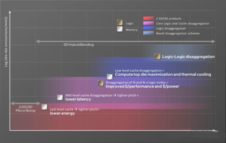
Figure 6. Advances in chip-to-chip bond spacing will enable caches, logic, and new disassembly schemes to achieve higher performance and power efficiency.
If the number of small chips increases and the bond spacing drops below 10um, standardized small-chip interfaces will be needed to produce known good chips for maximum package yield and rapid product verification and debug. Tighter packaging of more functional small chips presents challenges in power transfer, power density, and heat dissipation. Improved EDA system planning and modeling tools are needed to iterate through multiple package technology options to achieve the best system performance and cost balance of heat dissipation, power transfer, and small-chip-to-small-chip communication bandwidth.
Further innovation in EDA tools and design methodologies may be required to exploit the potential of fine-grained decomposition opportunities below ~2um chip-to-chip bond spacing. Today, most design methods and EDA tool approaches are optimized for a given silicon wafer, using a single homogeneous silicon technology. At the same time, fine-grained logic decomposition requires interoperability between multiple process design kits (PDKs), interface design for test function insertion tools, and upgrading of a wide range of signoff tools to handle multiple technologies simultaneously. Design methodologies for understanding swell process skew, voltage and temperature variations between multiple stacked chips with significantly different technologies need to be considered. Architects and technologists will have new opportunities to decompose subsections based on switching activity factors, leakage states, or other system-related performance metrics between different technologies. Potential optimization points across workloads, design points, packaging, and silicon technologies span more than is practical without widespread deployment of well-developed EDA tools and will likely rely on artificial intelligence and/or machine learning techniques across engineering functions.
4 Industry Collaboration for the Next 75 Years of Innovation
In the future, advanced packaging will play an increasing role in achieving power, performance, area, cost, time-to-market, design flexibility, and reliability. In addition, the expected timeline for scaling advanced packaging technologies will be compressed compared to past packaging transformations. To achieve maximum flexibility in creating 2.5D packages and 3D stacks, small chips from multiple foundries and suppliers should be able to be assembled seamlessly. To achieve this, the industry needs to adopt standard interfaces used by all small-chip designs and process nodes. In addition, current advanced 2.5D and 3D assembly technologies do not have standardized mechanical specifications, such as metallurgy, dielectric composition, and surface flatness. This makes it difficult to join small chips from different foundries, even if the electrical interface is standardized, i.e., UCIe. The industry needs to continue to work together to establish this standardization. In addition, assembly and test (AT) plants use too many carriers, pallets, and magazines for material and handling, resulting in inefficient labor and equipment. Industry-standard AT material carriers, equipment loading ports, and equipment front-end modules (EFEMS) need to be investigated to improve plant efficiency. Standardization is critical to reduce time to market for new packaging technologies in the open small-chip ecosystem.
The endless demand for lower power, lower latency and higher interconnect density and the need for tighter chip pitch scaling are driving the implementation of new architectures. As a result, wafer assembly tools will be needed that can align 3D stacked chips with nanometer interconnect pitch tolerances and run speeds to enable economically viable high-volume manufacturing. For finer features and denser interconnects, improved dimensional stability of the package substrate is required. Traditional organic packaging materials are sensitive to temperature variations that cause warpage during processing, which limits further scaling lithography on the typically large panels used during substrate fabrication, and new materials, technologies, and processing methods are needed to break this barrier.
Introducing power to the bottom of a 3D stack through highly resistive silicon via vias (TSVs) can lead to efficiency losses. Innovative power delivery solutions are needed to achieve sufficiently low parasitic and efficient power delivery to small chips in complex 3D stacks.
The lower logic chips in the 3D stack still generate heat and need to be cooled. Accurate, experimentally validated predictions of layout-based thermal performance requirements must be incorporated into the design engineering approach to ensure that all designs make the most efficient use of scaling. Effective cooling needs to be addressed through system design, package construction, materials, and process integration. Critical technologies, such as accurate metrology, rapid commissioning methods, and failure analysis techniques, are essential to success.
Power, heat and wiring constraints are bottlenecks to 3D-IC scaling. Across our industry, the technology development pipeline is rich in innovative ideas to address these challenges, including new transistors for density scaling (CFET, 2D); energy-efficient switches (tunneling FETs, FeFETs, spintronics); and advanced packaging technologies (with Cu and/or integrated photons) that allow heterogeneous integration of different technologies with low connection overhead, which can be be optimized independently or together within the package.
The industry may revisit III-V compound semiconductors (InGaAs/InP) for NMOS and Ge for PMOS because they have better electron and hole mobilities than Si and therefore enable more efficient circuit performance. These materials also have a smaller band gap, allowing transistors to switch efficiently at low voltages. Other innovations may include tunneling field effect and ferroelectric transistors. Examples of these devices have the potential to provide solutions for making more efficient transistors. Similarly, transistors based on 2D transition metal diols offer the potential for improved power performance regions. With the advent of STCOs, technologies are jointly optimized starting with workloads and applications, and the business case for these new technologies may be more viable than ever before, even though the initial product range of the new technologies is narrow, higher value can now be obtained.
To reduce the power consumed by migrating data between processing units and memory, the industry will need to consider computing near memory or within memory. The industry will need to develop new memory devices that are large enough but can be incorporated into integrated solutions that support logical devices. Neuromorphic computing is an example of a non-von Neumann type architecture that has the potential to leverage the integration of memory and logic. In addition, high-bandwidth optical interconnects that enable fast, long-distance data movement are critical for continued system scaling.
Finally, STCO will place new demands on future technical staff who, in addition to domain-specific expertise, will need interdisciplinary skills and knowledge to be able to fully integrate technologies at the system level.
5 Summary
The microtransistor, the cornerstone of the digital technology revolution, has transformed our society by opening up new industries, releasing human creativity, enabling amazing inventions and discoveries, influencing our society, and accelerating economic prosperity. After 75 years, its remarkable products and services are a testament to the innate human spirit of innovation, creativity, industry collaboration and entrepreneurship that has kept Moore's Law's quest for ever-increasing functionality alive. With semiconductor processing, the foundation of DTCO, and now STCO as an enhanced tool in the Moore's Law portfolio, the entire semiconductor industry will thrive by continually leveraging each other's unique strengths and valuable innovations. We look forward to the next 75 years of even more incredible human ingenuity!