Date:2022-09-02 11:49:46 Views:1025
Semiconductor materials with high thermal conductivity and high electron and hole mobilities are important for electronic and photonic devices and fundamental research. Among the ultra-high thermal conductivity materials, cubic boron arsenide (c-BAs: cubic boron arsenide) can theoretically reach both electron and hole mobilities of >1000 cm²/(Vs). Despite the spatial differences, we measured a thermal conductivity of 1200 W/(m-K) and a bipolar mobility of 1600 cm²/(Vs) at the same position of the cubic boron arsenide sample at room temperature using the optical transient grating technique. Calculations based on this showed that reducing the concentration of ionized impurities and neutral impurities is the key to obtaining high mobility and high thermal conductivity, respectively. The high bipolar mobility is accompanied by an ultra-high thermal conductivity.
In other words, cubic boron arsenide is expected to be a candidate material for next-generation electronics.

Semiconductor materials with both high electron and hole mobility and high thermal conductivity are beneficial for enhancing the performance of microelectronic and optoelectronic devices (1, 2). However, to date, materials with both high mobility and thermal conductivity have still not been identified. For example, the most widely used silicon (Si) and gallium arsenide (GaAs) have room temperature electron mobility of 1400 cm²/(VS) and 8500 cm²/(VS), respectively. However, their hole mobility (450 cm²/(VS) for Si, 400 cm²/(VS) for GaAs) and thermal conductivity (kRT=140 W/(m-K), 45 W/(m-K) for GaAs) at room temperature, this figure is lower than expected.
Although graphene has high electron and hole mobility and high in-plane thermal conductivity, its cross-plane thermal conductivity is low (3, 4). Although diamond has the highest RT thermal conductivity and excellent electron and hole mobilities, the forbidden band width of 5.4 eV makes it difficult to dope effectively by conventional means (5).
Recently, first-principles calculations have predicted that cubic boron arsenide has an extremely high room-temperature thermal conductivity (~1400 W/(m-K)), a figure that is 10 times higher than that of Si. This high value stems from its unusual phonon scattering and chemical bonding properties, which promote both weak three-phonon and four-phonon scattering. This prediction has now been confirmed experimentally, and the measured thermal conductivity of cubic boron arsenide in the kRT = 1000-1300 W/(m-K) range indicates that cubic boron arsenide is the most thermally conductive semiconductor material other than diamond.
First principles calculations also predict that cubic boron arsenide should have both high room temperature electron and hole mobilities, μe = 1400 cm²/(VS),μh = 2100 cm²/(VS). The main reason for such high electron and hole mobilities is the high energy and low occupation of polar optical phonons in cubic boron arsenide, which brings about weak carrier scattering. This property distinguishes cubic boron arsenide from other III-V semiconductor materials, which, with the exception of AlSb (μe=200 cm²/(VS) and μh= 400 cm²/(VS)), have high electron mobility but much lower hole mobility, where μe/μh>10 to ~100,.
Despite the excellent theoretical predictions, the high mobility of boron arsenide has not been confirmed from experimental measurements. Similar to the development history of other III-V semiconductors, the quality of cubic boron arsenide crystals is limited by a large and inhomogeneous defect density. Traditional bulk transport measurement methods are greatly limited by the defect density and do not provide access to the intrinsic properties of the material itself, and therefore the high defect density in cubic boron arsenide crystals hinders the validity of such measurements to assess the predicted high mobility.
Furthermore, previous studies have shown that there does not appear to be a strong correlation between thermal conductivity and electron mobility. kRT=186 W/(m-K) and μh predicted to be 400 cm²/(VS) for cubic boron arsenide microrod samples were measured by Kim et al. Chen et al. measured kRT=920 W/(m-K) and μh=22 cm²/( VS) millimeter-scale c-BAs crystals (millimeter-scale c-BAs crystals). The observed mobilities for both are much lower than the calculated mobilities and do not correlate significantly with the measured thermal conductivity. (The reasons for (i) the discrepancy between theoretical calculations and experiments and (ii) the decoupling between thermal and electrical properties have not been determined.
We measured the electrical mobility and thermal conductivity of a single crystal of cubic boron arsenide at the same point using an optical transient grating (TG) method. The experiments confirm that cubic boron arsenide has not only high thermal conductivity but also high electron and hole mobilities. According to theoretical calculations, ionizing impurities have a strong scattering effect on charge carriers, while neutral impurities mainly lead to a decrease in thermal conductivity. These findings make cubic boron arsenide the only known semiconductor with this desirable combination of properties and make it an ideal material for next-generation microelectronic applications.
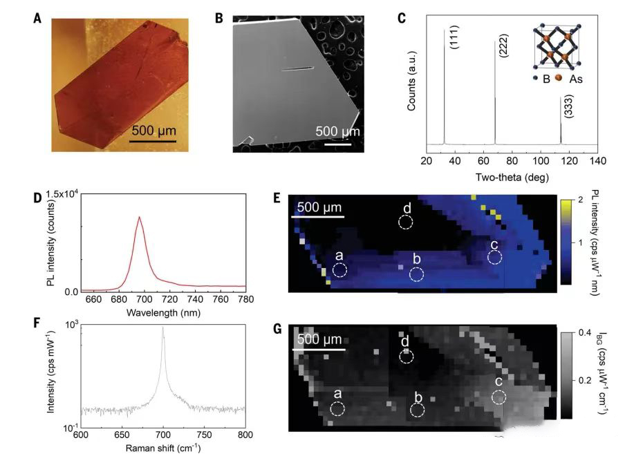
We prepared cubic boron arsenide samples (18) using multistep chemical vapor transport under different conditions (Figures S1 and S2). We used scanning electron microscopy (SEM) to image cubic boron arsenide single crystals with a thickness of about 20 μm (Fig. 1, a and B) and confirmed the cubic structure by x-ray diffraction (XRD) (Fig. 1C), in agreement with the literature (19).
We used photoluminescence (PL: photoluminescence) and Raman spectroscopy to determine the inhomogeneous impurity distribution in cubic boron arsenide (17, 20). We measured PL spectra (Fig. 1D) and performed two-dimensional (2D) PL mapping of cubic boron arsenide crystals (Fig. 1E). Local bright spots indicate spatial differences in charge carrier density and electron-hole complex dynamics. We also measured Raman spectra (Fig. 1F) and performed 2D Raman background scattering intensity (IBG) mapping (Fig. 1G). The strong Raman peak at about 700 cm-1 corresponds to the longitudinal optical (LO) mode at the center of the cubic boron arsenide region. the half-width of the LO peak and IBG can be attributed to mass disorder due to impurities, leading to large variations in thermal conductivity (11, 21).
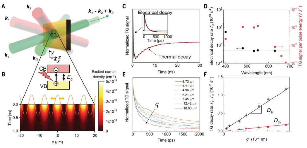
We used the TG technique (22-24) (Fig. 2A) to simultaneously measure electrical and thermal transport at multiple points (Fig. 1, circles a to d). Two femtosecond laser pulses (pumps) with wave vectors k1 and k2 produce sinusoidal optical interference on the cubic boron arsenide sample, which excites electron-hole pairs (Fig. S3). A third laser pulse (k3; probe) reaches the sample point after a delay time t and subsequently diffracts along the k1-k2+k3 direction and mixes with a fourth pulse (k4) used for outlier detection. The corresponding diffraction signal decays with time as the photoexcited carriers undergo diffusion and compounding. We show the calculated time-dependent electron-hole distribution in cubic boron arsenide in Figs. 2B and 2B. s4 and s5.

Fig. 1. Optical characterization of c-BAs single crystals. (A) Optical photograph. (B) SEM image. (C) XRD. a.u., arbitrary units; deg, degrees. (D and E) A typical PL spectrum (D) and 2D PL intensity mapping (E) integrated over 100-nm spectrum range for each spot. The dashed circles show TG measurement spots (a to d). cps, counts per second. (F and G) A typical Raman spectrum (F) and 2D mapping of background Raman scattering intensity (G) integrated over 100 cm−1 for each spot

Fig. 2. Thermal and electron transport measurements. (A) Schematic illustration of TG experiments. (B) Calculated time-dependent electron-hole pair density in c-BAs. CB, conduction band; VB, valence band; Eg, bandgap. (C) TG signal for c-BAs. Thermal conductivity is calculated from exponential fitting (red line). (D) Wavelengthdependent electrical decay rate Ge and TG peak amplitude. (E) TG signal with varying diffraction grating periods q. (F) Electrical decay rate (Ge) and thermal decay rate (Gth) versus q2 . Error bars show experimental uncertainties
The diffusion and complexation of the photoexcited carriers leads to a fast exponential decay of the TG signal (t < 1 ns), followed by a slower thermal decay (t > 1 ns) with opposite sign (Figure 2C). Short-time decay and long-time decay can be used to calculate the carrier mobility and thermal conductivity at the same point, respectively (see Figure S6 for details). The thermal conductivity is calculated directly by the exponential fit of the long-time decay (red line).
The electrical attenuation is sensitive to the wavelength of the pump pulse, and we used an optical parametric amplifier (OPA) to match the wavelength of the pump beam to the band gap of the cubic boron arsenide (2.02 eV) to avoid excitation of high-energy electrons, resulting in hot electrons and holes with different scattering kinetics and mobilities (25).
We also determined the wavelength-dependent electrical decay rate Γe and the lock-in amplifier amplitude of the TG peak (Fig. 2D). the TG decays faster at shorter wavelengths (<500 nm) and reaches a plateau near the band gap (~600 nm), followed by a signal loss of photon energy below the band gap (>650 nm) (Fig. S7).
The slopes of the electric decay Γe and thermal decay Γth with respect to q2 (Fig. 2, E and F) correspond to the bipolar diffusivity Da and thermal fusivity Dth of cubic arsenide. Da is subsequently converted into the bipolar mobility μa = eDa/kBT = 2μeμh/(μe+μh), which is mainly determined by the low mobility carriers, where kB is the Boltzmann constant, e is the fundamental charge, and T is the temperature.
From point a to point d, we measured a large number of room temperature thermal conductivities and bipolar mobilities (a: 920 W/(m-K) and 731 cm²/(VS); b: 1132 W/(m-K); 1482 cm²/(VS); d: 211 W/(m-K) and 328 cm²/(VS)). This large spatial variability in thermoelectric properties can be attributed to the corresponding variation in impurity density. Higher impurity density decreases the PL intensity and increases the IBG. to confirm this trend, we intentionally doped the cubic boron arsenide sample IV with carbon for thermal conductivity and bipolar mobility measurements ranging from k=200 to 953 W/(m-K) and μa=195 to 416 cm²/(VS), respectively, and also found large differences in IBG and low PL intensity (Figure 4) (S8 and S9).
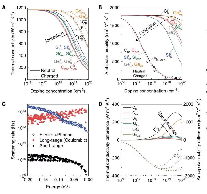
Common impurities in cubic arsenide are group IV elements such as C and Si. Due to the low formation energy, these impurities can be used as electron acceptors in cubic arsenide (26). The space charge generated by ionized impurities introduces distortions in the local bonding environment that drive specific phonon scattering mechanisms. The thermal conductivity of cubic boron arsenide can be calculated by solving the phonon Boltzmann transport equation, including three- and four-phonon scattering and phonon scattering from neutral (solid line) and charged (dashed line) group IV impurities on the B or As sites (27, 28) (Fig. 3A). We calculate k decreasing with increasing mass difference between the impurity and the host atom. On impurity ionization, the valence electron number of impurity (IV) matches that of B or As (III or V), leading to weaker bond perturbations (weaker bond perturbations) than that of the neutral impurity. Therefore, the reduction of thermal conductivity by ionized impurities is smaller than that by non-ionized impurities, especially when the substituted impurities have similar masses to the host atom, i.e. Ge-As and C+B .

Fig. 3. Theoretical calculation of the impurity effects on thermal conductivity and mobility. (A and B) Calculated thermal conductivity (A) and ambipolar mobility (B) with neutral (solid lines) and charged (dashed lines) group IV impurities. Open circles are mh values of bulk samples measured by electrical probes (fig. S12). (C) Calculated electron-phonon and short- and long-range impurity scattering rates for holes. Zero of energy is at the valence band maximum. Si– As ¼ 1018cm3. (D) Thermal conductivity (solid lines) and mobility (dashed lines) differences between charged and neutral impurities
Bond perturbation (bond perturbation) and Coulomb potential (Coulomb potential) of impurities have different effects on electron and hole transport kinetics in cubic boron arsenide. Based on recent advances in calculating the formation energy of charged impurities (29), we use ab initio calculations to investigate the effect of group IV impurities on the room temperature bipolar mobility of cubic boron arsenide (Fig. 3B). We show the electron-phonon scattering and long- and short-range defect scattering of holes in the contained cubic boron arsenide (see Fig. S10 for details) (Fig. 3C). Near the band edge, long-range Coulomb interactions with charged impurities are the dominant scattering mechanism. The lack of Coulomb potential of neutral impurities leads to weaker carrier scattering, causing μa to drop only at concentrations close to 1018 cm-3, when electron-neutral impurity scattering starts to show effects. However, the μa of charged impurities decreases significantly from 1016 cm-3 regardless of the impurity mass.
We elucidate the different effects of neutral and charged impurities on k and μa (Figure 3D). Compared to charged impurities, neutral impurities suppress k more strongly because of stronger bond perturbations (27). Due to Coulomb scattering, charged impurities mainly contribute to μa reduction regardless of mass. Charged impurities with masses similar to the main atom will exhibit room temperature thermal conductivity above 1000 W/(m-K) even at high impurity densities of 1019 cm-3 and a significant reduction of μa to below 400 cm²/(VS). Medium level 1018 cm-3.
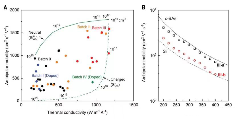
We can also highlight the trend of k and μa versus batches 0 to IV for neutral and charged impurities (Figure 4A and Table S1) (18). The solid and dashed lines in Fig. 4 show the μa and k trajectories calculated for neutral Si0 As and charged Si-As, respectively, from 1016 to 1020 cm-3. The scattering points are the measured μa and k values for different batches of samples, marked with different colors. All measured data were fitted to the region between the trajectory curves.
In the high quality cubic boron arsenide batch (III), we measured μa = 1600 ± 170 cm²/(VS) and k = 1200 ± 130 W/(m-K). We also measured the temperature dependent μa for two different points (III-a and III-b) of the high quality samples (Figure S11), and the measured μa for III-a agrees with the calculated results (Figure 4B). Hall measurements of the bulk samples (the bulk samples) provide μh and carrier concentration p, which has spatially varying impurity concentrations over the entire sample. The measured bulk μh plotted in Figure 3B (see Figure S12 for details) is limited by the average impurity concentration rather than the local point of low impurity content.

Fig. 4. Ambipolar mobility and thermal conductivity of c-BAs. (A) Measured mobility and thermal conductivity of c-BAs from different batches (batches 0, I, II, III, and IV). See table S1 for details. The solid and dashed lines show the calculated ma and k with varying concentrations of neutral Si0 As and charged Si– As, respectively. Typical uncertainties for ma and k are 11%. (B) Temperaturedependent ambipolar mobility of c-BAs (III-a and III-b). The solid and dashed lines show calculated ma of pristine c-BAs and Si, respectively (32).
The high spatial resolution thermogravimetric measurements provide clear evidence for the presence of both high electron and hole migration in cubic boron arsenide and suggest that by eliminating defects and impurities, cubic boron arsenide can exhibit high thermal conductivity and high electron and hole migration. Furthermore, the weak correlation observed between the local thermal conductivity and mobility is caused by the different effects of neutral and ionized impurities on these quantities. This remarkable combination of electronic and thermal properties, along with thermal expansion coefficients and lattice constants that closely match those of common semiconductors such as Si and GaAs (30,31), makes cubic arsenide a promising material for integrating current and future semiconductor fabrication processes and capable of addressing the challenges of next-generation electronics in terms of thermal management.
References and Notes
1. X. Qian, J. Zhou, G. Chen, Nat. Mater. 20, 1188–1202 (2021).
2. G. Chen, Nat. Rev. Phys. 3, 555–569 (2021).
3. K. S. Novoselov et al., Science 306, 666–669 (2004).
4. A. A. Balandin et al., Nano Lett. 8, 902–907 (2008).
5. C. J. H. Wort, R. S. Balmer, Mater. Today 11, 22–28 (2008).
6. L. Lindsay, D. A. Broido, T. L. Reinecke, Phys. Rev. Lett. 111, 025901 (2013).
7. D. A. Broido, L. Lindsay, T. L. Reinecke, Phys. Rev. B 88, 214303 (2013).
8. T. L. Feng, L. Lindsay, X. L. Ruan, Phys. Rev. B 96, 161201 (2017).
9. J. S. Kang, M. Li, H. Wu, H. Nguyen, Y. Hu, Science 361, 575–578 (2018).
10. F. Tian et al., Science 361, 582–585 (2018).
11. S. Li et al., Science 361, 579–581 (2018).
12. T. H. Liu et al., Phys. Rev. B 98, 081203 (2018).
13. D. L. Rode, Phys. Rev. B 3, 3287–3299 (1971).
14. A. Nainani, B. R. Bennett, J. B. Boos, M. G. Ancona, K. C. Saraswat, J. Appl. Phys. 111, 103706 (2012).
15. J. I. Pankove, T. D. Moustakas, Semicond. Semimet. 50, 1–10 (1997).
16. J. Kim et al., Appl. Phys. Lett. 108, 201905 (2016).
17. X. Chen et al., Chem. Mater. 33, 6974–6982 (2021).
18. Materials and methods are available as supplementary materials online.
19. J. A. Perri, S. Laplaca, B. Post, Acta Cryst. 11, 310 (1958).
20. S. Yue et al., Mater. Today Phys. 13, 100194 (2020).
21. A. Rai, S. Li, H. L. Wu, B. Lv, D. G. Cahill, Phys. Rev. Mater. 5, 013603 (2021).
22. A. A. Maznev, T. F. Crimmins, K. A. Nelson, Opt. Lett.
23, 1378–1380 (1998). 23. A. A. Maznev, K. A. Nelson, J. A. Rogers, Opt. Lett. 23, 1319–1321 (1998).
24. S. Huberman et al., Science 364, 375–379 (2019).
25. K. Chen et al., Carbon 107, 233–239 (2016).
26. J. L. Lyons et al., Appl. Phys. Lett. 113, 251902 (2018).
27. M. Fava et al., Npj Comput. Mater. 7, 54 (2021).
28. M. Fava et al., How dopants limit the ultrahigh thermal conductivity of boron arsenide: A first principles study, version 1, Zenodo (2021); https://doi.org/10.5281/zenodo.4453192.
29. C. Freysoldt et al., Rev. Mod. Phys. 86, 253–305 (2014).
30. F. Tian et al., Appl. Phys. Lett. 114, 131903 (2019).
31. X. Chen et al., Phys. Rev. Appl. 11, 064070 (2019). 32. N. D. Arora, J. R. Hauser, D. J. Roulston, IEEE Trans. Electron Dev. 29, 292–295 (1982).