Date:2022-08-15 11:35:25 Views:963
When baking a cake, it's hard to know when the oven will be in the state we want it to be. For microelectronic chips, the stakes are even higher: How can engineers be sure that the inside of the chip is exactly as the designer intended? How can semiconductor design companies determine whether their intellectual property has been stolen? More worryingly, who can be sure that there are no self-destruct switches or other hardware Trojans secretly embedded?
Currently, probing is done by grinding off each layer of the chip and examining it with an electron microscope. This process is slow and certainly destructive, making this method hardly satisfactory.
Levi, the author of this article, studies semiconductors and Aeppli studies X-rays. So, after careful consideration of the problem, we considered using X-rays for nondestructive imaging of chips. Although the resolution we needed was beyond that of a medical X-ray scanner, it was clear to us that such resolution was possible. Thus, our "chip scanning" project was born.
In a few years, we will be able to map the complete interconnect structure of even the most advanced and complex processors without destroying them. Currently, the process takes more than a day, but improvements in the next few years should allow the entire chip to be mapped in a few hours.
The technique, called "stacked X-ray layered imaging" (PyXL), requires the use of the world's most powerful X-ray light source. However, most of these facilities happen to be conveniently located near where many advanced chip designs are made. So, with the popularity of this technology, there is no way to hide from any defects, malfunctions or complex shenanigans.
Having decided to adopt this approach, our first task was to determine what the state-of-the-art X-ray technology could do. This work was done at the Paul Scherrer Institute (PSI) in Switzerland, where Eppley works. The Paul Scherrer Institute in Switzerland is home to the Swiss Light Source (SLS) synchrotron, one of the 15 brightest coherent X-ray sources built to date.
Coherent X-rays differ from X-rays used in medical or dental clinics in that the difference is akin to a highly collimated beam from a laser pointer versus an incandescent light bulb emitting light in all directions.
The Swiss Light Source and similar facilities first accelerate electrons to near the speed of light, resulting in a highly coherent beam of x-ray photons. A magnetic field then deflects these electrons to produce the desired X-rays.
To see what could be done with the Swiss Light Source, our interdisciplinary team purchased an Intel Pentium G3260 processor from a local store for about $50 and removed the package to expose the silicon chip. The CPU was manufactured using 22nm complementary metal oxide semiconductor (CMOS) finned field effect transistor (FinFET) technology.
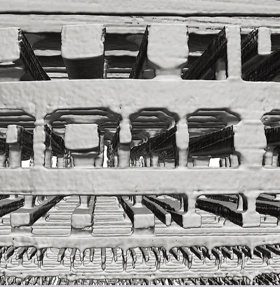
Like all such chips, the G3260's transistors are made of silicon, but it is the arrangement of metal interconnects that connects them together to form the circuit. With more than 15 layers of interconnects, the interconnects in modern processors look like a city street grid map when viewed from above. The lower layers closer to silicon are incredibly finely constructed, separated by just a few nanometers in today's most advanced chips. The interconnect layers get sparser and more spaced as you go up until you reach the top layer, where electrical contact pads connect the chip to its package.
We cut a 10-micron-wide cylinder from the G3260 and began our inspection. This destructive step was taken because it greatly simplified the problem. 10 microns is less than half the depth of photon penetration of the Swiss Light Source, so with something so small, we could detect enough photons passing through the base column to determine the internal conditions.
We placed the sample on a mechanical carrier table, allowed it to rotate around its cylindrical axis, and then emitted a beam of coherent X-rays from the side. As the sample rotated, we illuminated it with an overlapping 2 µm wide dot pattern.
At each illumination point, coherent X-rays are diffracted as they pass through the chip's curved interconnecting copper towers, projecting the pattern onto the detector, where it is stored for subsequent processing. The recorded projection contains enough information about the material through which the X-rays pass to determine its three-dimensional structure. This method is called "stacked X-ray computed tomography" (PXCT). Superposition imaging is a computational process that produces an image of an object by means of an interference pattern of light.
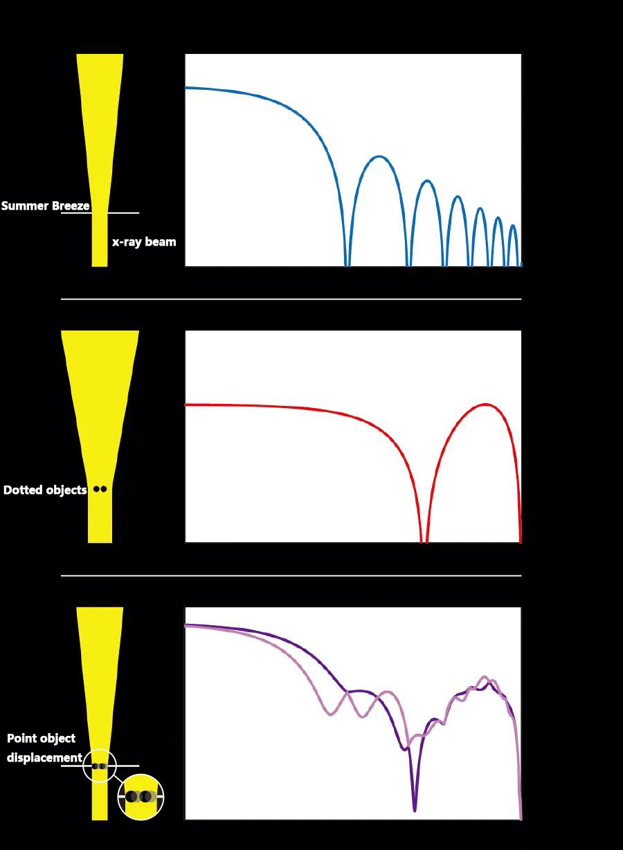
The basic principle of PXCT is relatively simple and is similar to the diffraction of light through a gap. You may remember from your introductory physics class that if you shine a coherent beam of light through a slit onto a plane at a distance, a Fraunhofer diffraction pattern is produced. This is a light and dark band pattern, or streak pattern, whose spacing is proportional to the ratio of the wavelength of the light to the width of the slit.
If instead of shining light through the slit, you shine it on a pair of closely spaced objects that are so small that they actually look like dots, then you will get a different pattern. The position of the objects in the beam does not matter. As long as they remain the same distance from each other, you can move them and will get the same pattern.
While neither phenomenon by itself will allow you to reconstruct the intricate interconnections in the microchip, if you combine them, you will understand the principle. Putting the pair of objects into the slit produces an interference pattern resulting from the diffraction formed by the combination of the slit and the objects, which reveals information about the width of the slit, the distance between the objects, and the relative positions of the objects and the slit. If the two points are moved slightly, the interferogram will be shifted. It is through this displacement that we can accurately calculate the position of the object in the slit.
Any real sample can be considered as a set of point-like objects, producing a complex X-ray scattering pattern. Such patterns can be used to infer the arrangement of these point-like objects in two-dimensional space. Using this principle, we can image the object in three dimensions by rotating the sample in the beam, a process called "tomographic reconstruction".
To map the structure at the desired resolution, it is necessary to ensure that enough data is collected. The resolution is determined by the X-ray wavelength, detector size and a number of other parameters. Our initial measurements with the Swiss Light Source used X-rays at a wavelength of 0.21 nanometers, and the detector had to be placed about 7 meters from the sample to achieve the target resolution of 13 nanometers.
In March 2017, we published some very nice, 3D images of copper wire interconnects in the Intel Pentium G3260 processor, demonstrating the use of PXCT for nondestructive imaging of integrated circuits.
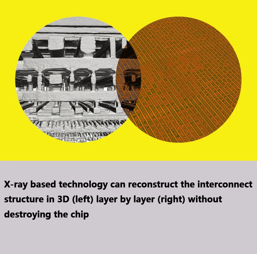
These images reveal the 3D characteristics and complexity of the electrical interconnects in this CMOS integrated circuit. Also, the images capture interesting details such as defects in the metal connections between the layers and the roughness between the copper and its surrounding silica dielectric.
This proof-of-principle demonstration alone shows the potential of the technology for failure analysis, design verification and quality control. Therefore, similarly sized cylinders were cut from chips fabricated using other companies' technologies and probed using PXCT. The resulting 3D reconstruction details resembled fingerprints, details that are unique to integrated circuits and reveal the chip manufacturing process.
The early successes achieved encouraged us. However, we knew we could do better, and we could build a new type of X-ray microscope and come up with a more efficient way to use chip design and manufacturing information to improve image reconstruction. We call this new technique "stacked X-ray layered imaging" (PyXL).
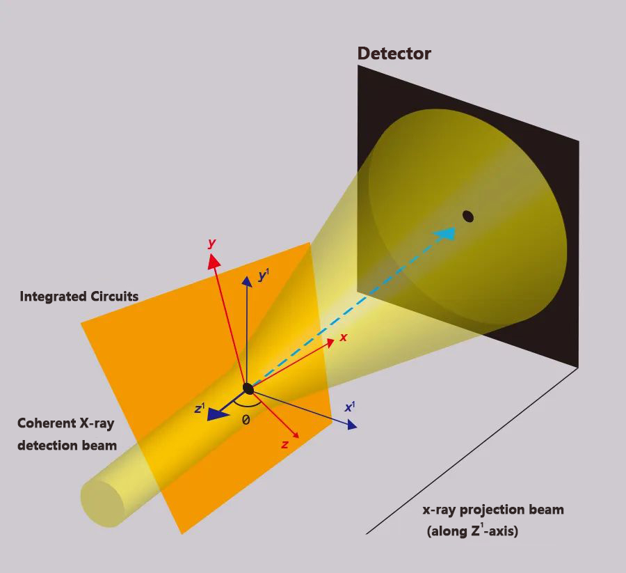
The first problem to be solved is how to scan an entire 10 mm wide chip when the X-ray penetration depth is only about 30 µm. To solve this problem, we first tilted the chip at an angle with respect to the beam.
Next, we rotated the sample around an axis perpendicular to the plane of the chip. At the same time, we also moved the sample laterally in a raster fashion. In this way, all areas of the chip were scanned with the beam.
During this process, the X-rays passing through the chip are scattered by the material inside the IC at all times, creating a diffraction pattern. As with PXCT, the diffraction pattern from the overlapping illumination points contains redundant information about the passage of X-rays. The imaging algorithm then infers the structure that is most consistent with all measured diffraction patterns. Using this information, we can then reconstruct the 3D internal structure of the entire chip.
Of course, there are many issues to consider in order to develop a new type of microscope. It must have a stable mechanical design, including a precise moving carrier stage and position measurement. It must also record in detail how the beam illuminates each point on the chip and the subsequent diffraction pattern that is produced. Finding practical solutions to these and other problems required the combined efforts of a team of 14 engineers and physicists. the geometry of PyXL also required us to develop new algorithms to interpret the data collected. It was a tough job, but by the end of 2018, we had successfully probed the 16nm IC and published the results in October 2019.
In these experiments, we used PyXL to virtually strip each layer of interconnects to reveal the circuits they form. In early tests, we inserted a small defect in the design file for the interconnect layer closest to the silicon. When we compared this version of the interconnect layer to the chip reconstructed using PyXL, the defect immediately became apparent.
In principle, with respect to integrated circuits, even those manufactured with state-of-the-art equipment, we only need a few days of work to use PyXL to obtain useful information about their integrity. The interconnections inside today's cutting-edge processors are separated by only a few tens of nanometers, and our technique can, at least in principle, produce images of structures smaller than 2 nanometers.
However, it does take longer to improve resolution. Although we have built hardware capable of scanning areas up to 1.2 cm x 1.2 cm in full at the highest resolution, it is impractical to do so. Zooming in on the region of interest would be a better use of time. In our initial experiments, a low-resolution (500 nm) scan of a square area on a chip 0.3 mm thick on one side took 30 hours. A high-resolution (19 nm) scan of a much smaller area on the chip (only 40 µm wide) took 60 hours.
The imaging rate is essentially limited by the X-ray flux available to us at the Swiss Light Source. But other facilities have much higher X-ray fluxes, and methods are being investigated to increase the "brightness" of the X-ray source, that is, the combination of the number of photons produced, the beam area and its propagation speed. For example, the MAX IV laboratory in Lund, Sweden, has pioneered a method to increase its brightness by two orders of magnitude. It can also be improved by one or two orders of magnitude with new X-ray optics methods. Combined with these improvements, the total flux will one day be 10,000 times higher.
With this higher flux, we should achieve 2 nm resolution in less time than it takes to achieve 19 nm resolution today. Our system can also measure a 1-square-centimeter integrated circuit, the size of an Apple M1 processor, in 30 hours at 250-nm resolution.
There are also other ways to improve the imaging speed and resolution, such as more stable detection of the beam and improving our algorithms to account for the design rules of the integrated circuit and the distortion that can result from high X-ray exposure.
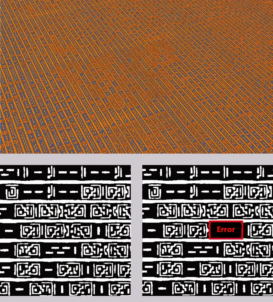
We can already learn a lot about the interconnect layout of an integrated circuit now, and with further improvements we should be able to understand it fully, including the materials it uses. 16nm technology nodes include copper, aluminum, tungsten and compounds called silicides. We can even make local measurements of the strain in the silicon lattice that comes from the multilayer manufacturing processes used to make cutting-edge devices.
Copper interconnect technology is approaching its limits, so identifying the material may be especially important. In contemporary CMOS circuits, copper interconnects are susceptible to electromigration, where currents kick copper atoms out of aligned queues and create voids in the structure. To counter this, interconnects are encased in barrier materials. But these sheaths can be so thick that they leave little room for copper, resulting in interconnects with too high a resistance. As a result, alternative materials such as cobalt and ruthenium are being explored. The interconnects we are talking about are so fine that resolutions of less than 10 nanometers are needed to distinguish them from each other.
There is reason to believe that the goal will be achieved. To support the construction of new and upgraded X-ray sources, researchers around the world are proposing to apply PXCT and PyXL to hardware and wetware (the brain) "linkers", which is one of the key arguments. Meanwhile, our labs in California and Switzerland are still working on developing better hardware and software. So in the near future, if you're wondering about your new CPU, or curious about a competitor's CPU, you can take a "fly-through" tour of its inner workings to make sure everything works.