Date:2022-08-12 11:06:25 Views:1321
Probably the most far-reaching technological achievement of the last 50 years has been the steady march of transistors to smaller, as always, bringing them closer together and reducing their power consumption. However, ever since the author began his career at Intel more than 20 years ago, we have been hearing the alarm - that the decline of transistors to infinity is coming to an end. Yet, year after year, brilliant new innovations continue to drive the semiconductor industry further.
In the process, our engineers have had to change the architecture of transistors so that we can continue to shrink area and power consumption while improving chip performance. This is what drove us to replace the "flat" transistor designs that were popular in the second half of the 20th century with 3D finned devices in the first half of the 2010s. Now, FinFETs also have an end date, and a new all-around (GAA) structure will soon be in production.
But we have to look beyond that, because even with this new transistor architecture (which Intel calls RibbonFET), there are limitations to our ability to shrink the size.
So, when will we move to the future of scaling? We will continue to focus on the third dimension. We have created experimental devices stacked on top of each other that offer logic scaled down by 30% to 50%. Crucially, the top and bottom devices are of two complementary types, NMOS and PMOS, which have been the basis of all logic circuits for the last few decades. We believe that this 3D stack of complementary metal oxide semiconductors (CMOS) or CFETs (complementary field effect transistors) will be the key to extending Moore's Law into the next decade.
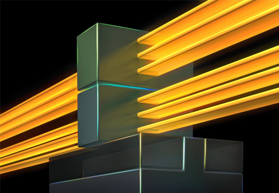
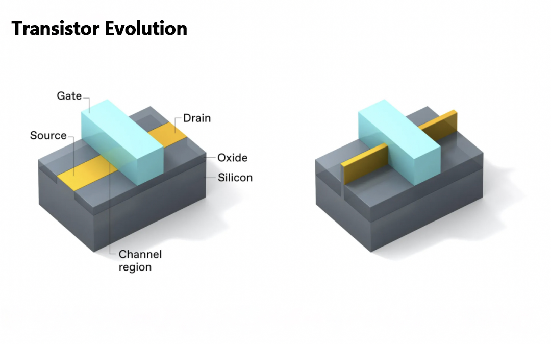
Transistor Evolution
Continuous innovation is an important foundation of Moore's Law, but each improvement requires trade-offs. To understand these trade-offs and how they inevitably lead us to 3D stacked CMOS, you need some background knowledge about how transistors work.
Every metal oxide semiconductor field effect transistor or MOSFET has the same basic set of components: the gate stack, the channel region, the source, and the drain. The source and drain are chemically doped so that they are either rich in mobile electrons (n-type) or lack them (p-type). The channel region has the opposite doping of the source and drain.
In the planar versions of transistors used in advanced microprocessors until 2011, the gate stack of MOSFETs is located directly above the channel region and is designed to project an electric field into the channel region. Applying a large enough voltage to the gate (relative to the source) creates a layer of moving charge carriers in the trench region, allowing current to flow between the source and drain.
As we narrow down the classical planar transistor, something that device physicists call the "short-channel effect" has attracted a lot of attention. Basically, it's because the distance between source and drain becomes so small that current leaks through the channel when it shouldn't, largely due to the gate electrode's difficulty in depleting the channel of charge carriers. To solve this problem, the industry has turned to a completely different transistor architecture, the FinFET, which wraps the gate around the trench on three sides to provide better electrostatic control.
Intel introduced its FinFET at the 22nm node in 2011 and used it for its third-generation Core processors, and the transistor architecture has been a Moore's Law mainstay ever since. With FinFET, we can also run at lower voltages and still have less leakage, reducing power consumption by about 50 percent at the same performance level as the previous-generation planar architecture. finFET also has faster switching and a 37 percent performance improvement. And because conduction occurs on both vertical sides of the "Fin," the device can drive more current through a given area of silicon than a planar device that only conducts along one surface.
However, we do lose something when we move to FinFETs. In planar devices, the width of the transistor is defined by photolithography, so it is a highly flexible parameter. But in FinFETs, the transistor width comes in the form of discrete increments - adding fins one at a time - a feature commonly referred to as fin quantization. quantization.) As flexible as FinFETs may be, fin quantization is still an important design constraint. The design rules surrounding it and the desire to add more fins to improve performance increase the overall area of the logic cell and complicate the interconnect stack that turns a single transistor into a complete logic circuit. It also increases the capacitance of the transistor, which reduces some of its switching speed. So while FinFETs have served us well as an industry workhorse, a new, more refined approach is still needed.
In the RibbonFET, the gate surrounds the transistor channel region for enhanced control of the charge carriers. The new structure also allows for better performance and finer optimization.
These requirements led to the creation of the new transistor architecture RibbonFET, 11 years after the introduction of the FinFET. In it, the gate is completely surrounding the channel, providing tighter control of the charge carriers within the channel, which are now formed by nanoscale silicon strips. Using these nanoribbons (also called nanosheets), we can again use lithography to vary the width of the transistor as needed.
Removing the quantization constraint allows us to generate the right size width for the application. This allows us to balance power, performance and cost. More importantly, by stacking and operating the Ribbon in parallel, the device can drive more current and increase performance without increasing the device area.
Intel believes RibbonFET is the best choice for achieving higher performance at reasonable power, and they will introduce this transistor architecture on the Intel 20A manufacturing process to be introduced in 2024, accompanied by innovations such as Intel's backside power technology, PowerVia.
Stacked CMOS
One thing that the planar, FinFET, and RibbonFET transistors have in common is that they all use CMOS technology, which, as mentioned above, consists of n-type (NMOS) and p-type (PMOS) transistors. CMOS logic became mainstream in the 1980s because it consumed significantly less current than alternative technologies, especially NMOS-only circuits. Less current also led to higher operating frequencies and higher transistor densities.
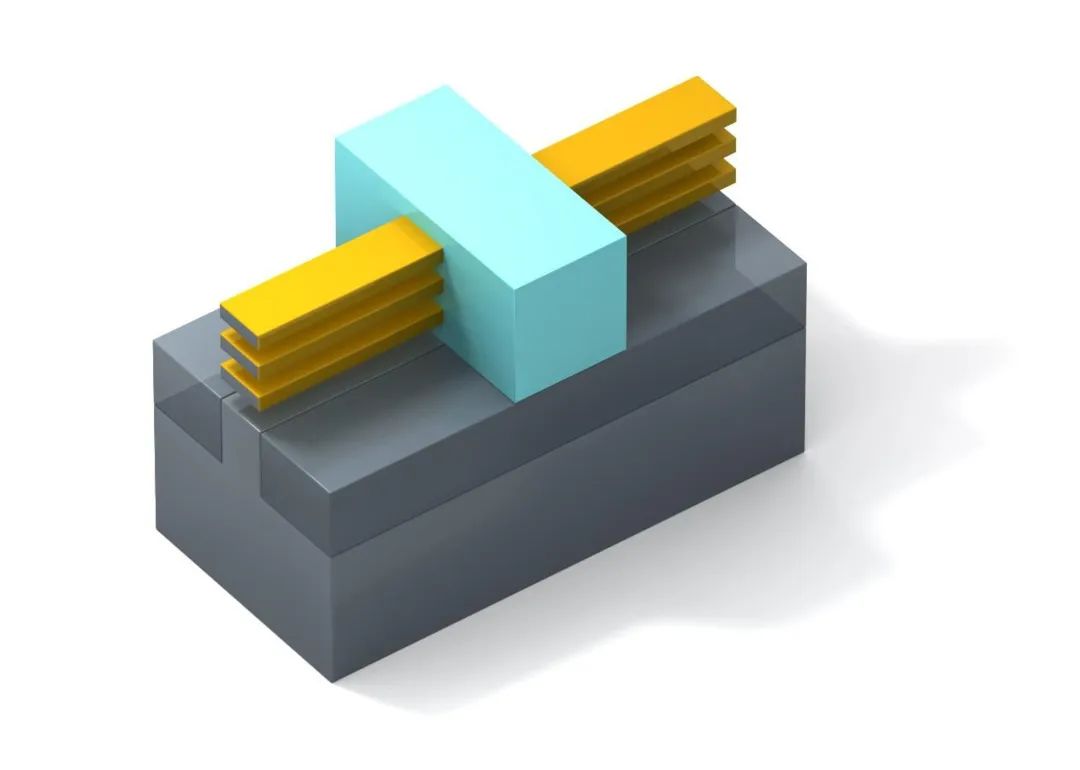
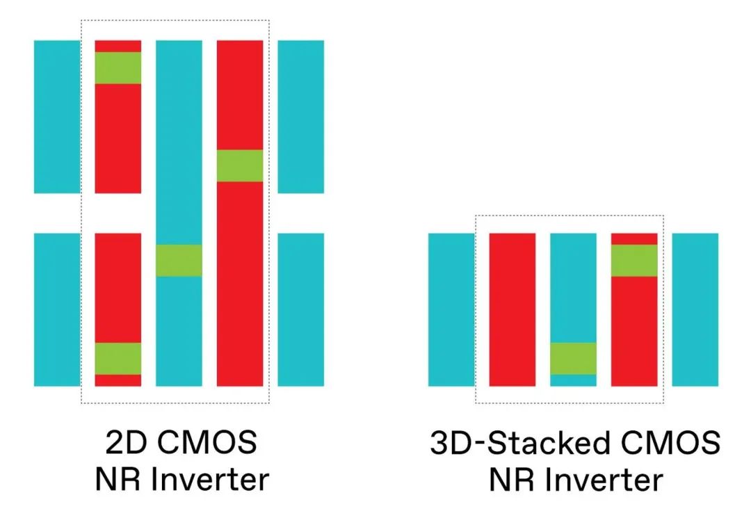
To date, all CMOS technologies have placed standard NMOS and PMOS transistor pairs side-by-side. But in a keynote at the 2019 IEEE International Electron Devices Conference (IEDM), Intel introduced the concept of 3D stacked transistors that place NMOS transistors on top of PMOS transistors. The following year, at IEDM 2020, Intel demonstrated the first design of a logic circuit using this 3D technology, the inverter. combined with proper interconnects, the 3D stacked CMOS approach effectively halves the inverter footprint and doubles the area density, further pushing Moore's Law of Moore's Law.
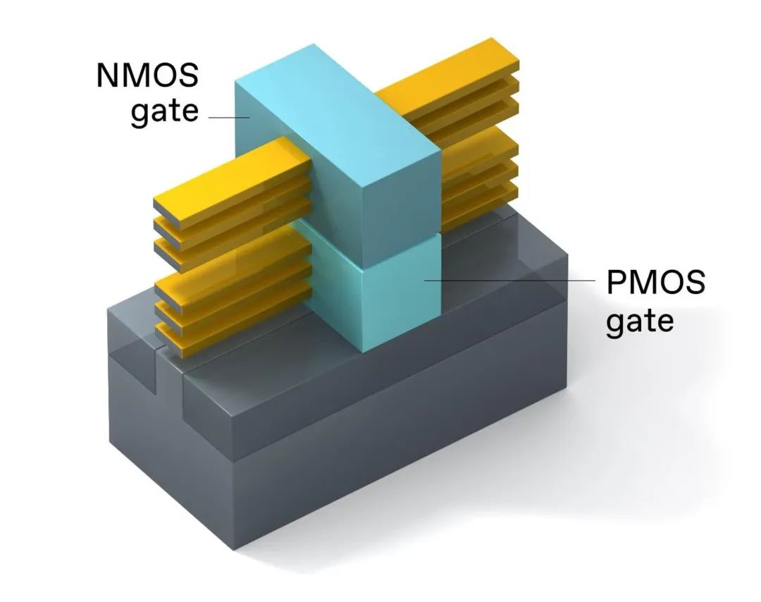
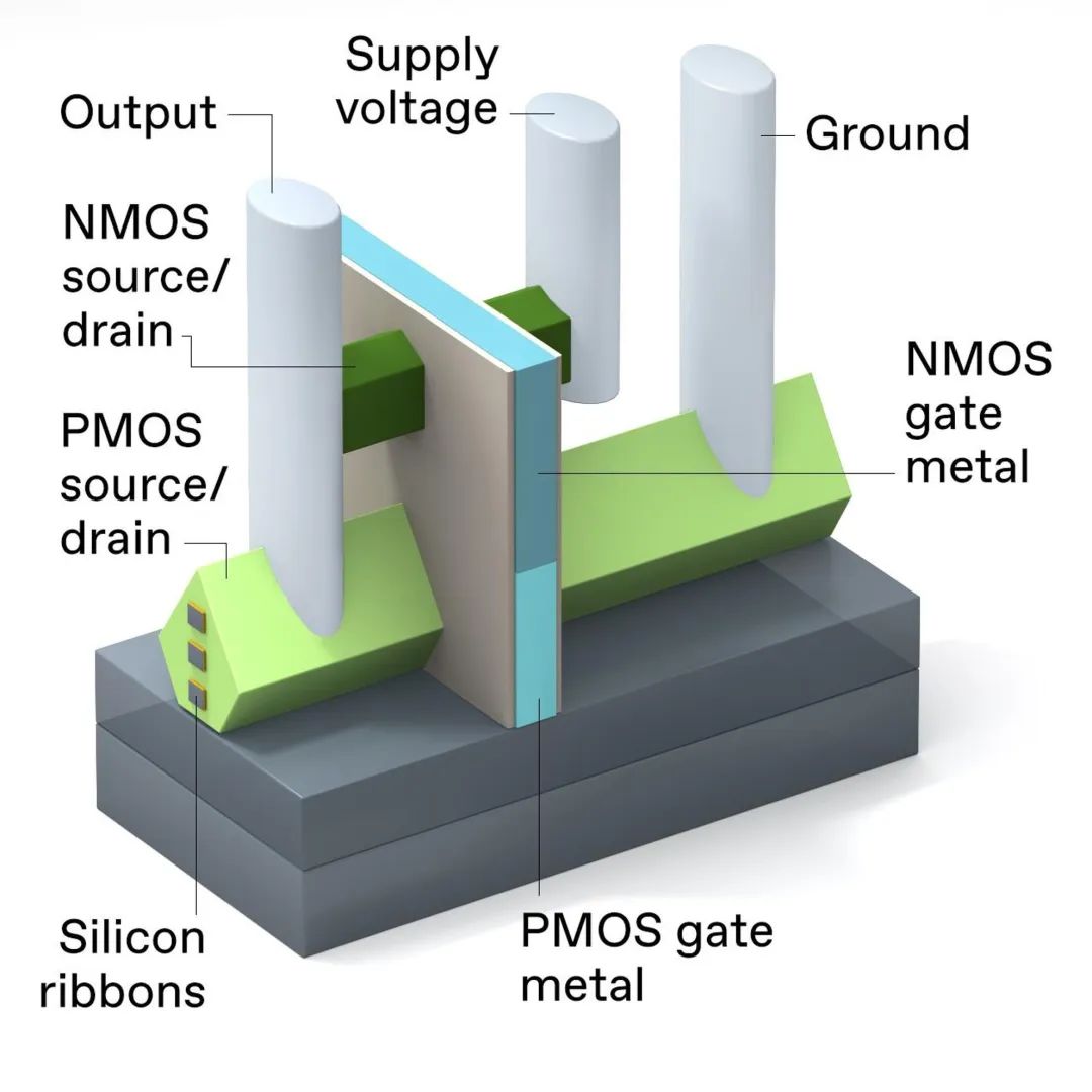
3D stacked CMOS places a PMOS device on top of an NMOS device in the same footprint as a single RibbonFET, using different metals for the NMOS and PMOS gates.
Taking advantage of the potential benefits of 3D stacking means solving many process integration challenges, some of which will stretch the limits of CMOS manufacturing.
Intel has built a 3D stacked CMOS inverter using a so-called self-aligned process, where both transistors are built in a single manufacturing step. This means building the n-type and p-type source and drain by epitaxy (crystal deposition) and adding different metal gates to the two transistors. By combining the source-drain and bimetal gate processes, Intel was able to create silicon nanoribbons of different conductivity types (p-type and n-type) to form stacked CMOS transistor pairs. The design also allows us to adjust the device's threshold voltage - the voltage at which the transistor begins to switch - for the top and bottom nanoribbons, respectively.
In CMOS logic, NMOS and PMOS devices are typically placed side-by-side on the chip. Early prototypes stacked NMOS devices on top of PMOS devices, thereby compressing the circuit size
How did Intel do it all?
Self-aligning 3D CMOS manufacturing starts with a silicon wafer. On this wafer, Intel deposited duplicate layers of silicon and silicon-germanium, a structure called a superlattice. Intel then uses a photolithography pattern to cut part of the superlattice and leave a fin-like structure. The superlattice crystal provides a strong support structure for what happens later.
Next, Intel deposits a "virtual" (dummy) piece of polysilicon on top of the portion of the superlattice where the device gates will go to protect them from the next step in the process. This step, called the vertically stacked dual source/drain process, grows phosphorous-doped silicon at the ends of the top nanoribbon (future NMOS devices) while selectively growing phosphorous-doped silicon on the bottom nanoribbon (future PMOS devices) (boron-doped silicon germanium) on the bottom nanoribbon (future PMOS device). After this step, Intel deposits dielectrics around the source and drain to electrically isolate them from each other, and then polishes the wafer to perfect flatness.
Side view of a 3D stacked inverter showing the complexity of its connections
Finally, the gate is constructed.
First, we remove the virtual gate we placed earlier to expose the silicon nanoribbon. Next we etch away just the silicon germanium, releasing a stack of parallel silicon nanoribbons, which will be the channel area of the transistor. We then apply a thin layer of insulator, which has a high dielectric constant, to all sides of the nanoribbons. The nanoribbon channels are so small and positioned in such a way that we cannot chemically dope them as effectively as we can with planar transistors. Instead, we use the metal gates property called work function to give the same effect. We use one metal around the bottom nanoribbon to form the p-doped channel and another metal around the top nanoribbon to form the n-doped channel. Thus, the gate stack is complete and the two transistors are finished.
This process may seem complicated, but it's better than the alternative technique - a technique called sequential 3D stacking CMOS. With this method, NMOS devices and PMOS devices are built on separate wafers, the two are bonded, and the PMOS layer is then transferred to the NMOS wafer. In contrast, the self-aligning 3D process requires fewer manufacturing steps and tighter control of manufacturing costs, a technique Intel demonstrated in research and reported at IEDM 2019.
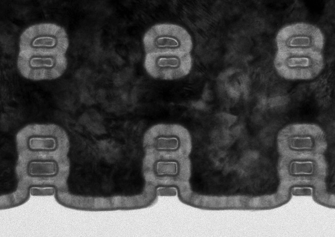
By stacking NMOS on top of PMOS transistors, 3D stacking effectively doubles the density of CMOS transistors per square millimeter, although the actual density depends on the complexity of the logic cells involved. inverter cells are shown from above, indicating source and drain interconnects [red], gate interconnects [blue], and vertical connections [green]
Importantly, the self-alignment approach also avoids the potential for misalignment problems when bonding two silicon wafers. Nevertheless, sequential 3D stacking is being explored to facilitate the integration of silicon with non-silicon channel materials, such as germanium and III-V semiconductor materials. These methods and materials may become relevant as Intel looks to tightly integrate optoelectronics and other functions on a single chip.
The new self-aligning CMOS process and the 3D stacked CMOS it creates are working well and seem to have a lot of room for further miniaturization. At this early stage, this is very encouraging. Devices with 75 nm gate lengths demonstrate low leakage with excellent device scalability and high on-state current. Another promising sign: Intel has fabricated wafers with a minimum distance between two stacked devices of just 55 nm. While the device performance results it obtained are not documented per se, they do compare to a single non-stacked control device built on the same wafer and with the same processing.
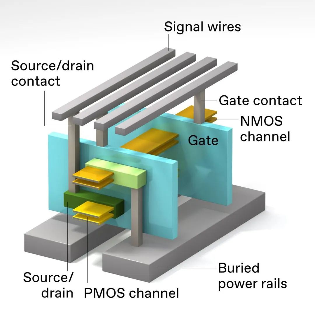
Making all the required connections to the 3D stacked CMOS is a challenge. Power connections need to be made from the bottom of the device stack. In this design, the NMOS device [top] and the PMOS device [bottom] have separate source/drain contacts, but both devices have a common gate
Along with process integration and experimental work, Intel is conducting many theoretical, simulation and design studies to gain insight into how best to use 3D CMOS. through these, Intel has discovered some key considerations in transistor design. Notably, we now know that we need to optimize the vertical pitch between NMOS and PMOS - because if it's too short it increases parasitic capacitance, but if it's too long it increases the resistance of the interconnect between the two devices. Either extreme will result in a slower circuit consuming more power.
Many design studies (such as one presented at IEDM 2021 by the TEL Research Center in the US) focus on providing all the necessary interconnects in the limited space of 3D CMOS and doing so without significantly increasing the area of the logic cells they form. the TEL study shows that there are many opportunities for innovation in finding the best interconnect options. The study also highlights that 3D stacked CMOS will require interconnects both above and below the device. This option, called a buried power rail, uses interconnects that power the logic cells but do not transfer data, and moves them to the silicon below the transistors. Intel's PowerVIA technology, which does just that, is scheduled to be available in 2024 and will therefore play a key role in enabling the commercialization of 3D stacked CMOS.
The Future of Moore's Law
With RibbonFET and 3D CMOS, Intel has a clear path to extend Moore's Law beyond 2024. In a 2005 interview, when asked to reflect on what made his law possible, Gordon Moore admitted to "being surprised from time to time at how we were able to make progress. There were times in the process when I thought we had reached the end of the road and things were dwindling, but our creative engineers came up with solutions."
With the shift to FinFETs, the optimizations that came with them, and now the development of RibbonFETs and eventually 3D stacked CMOS, and the myriad package improvements that surround them to support them, we think Mr. Moore will be surprised again.


Phone:+86-137-5112-7429
Email:sales@hyx-tech.com
Address:14D2, block A, Modern window building,ZhenHua Road,Futian District, Shenzhen
 sales@hyx-tech.com
 +86-0755-2399-7487
 sales@hyx-tech.com
 Login
Login Register