Date:2022-08-08 10:13:16 Views:1102
Although the vast majority of the semiconductor market is occupied by mature processes, most applications do not need to use more advanced 2nm process, but the companies are still competing to chase, and even recently rumored that the two major semiconductor countries to jointly develop 2nm chip news. The "2nm phenomenon", it is worth thinking about.
Advanced process market share rise
It is not difficult to see, although the semiconductor market is now occupied by mature processes, but the advanced process is pivotal.
With the continuous development of Moore's Law, the road of development of advanced processes is full of thorns. Therefore, as the technology development becomes more and more difficult, many manufacturers have chosen to give up the competition of advanced process and completely devote themselves to the development of mature process. For example, wafer foundry Gecko had publicly said in 2020 to give up the competition below 7nm.
However, as people's pursuit of emerging technologies continues to accelerate, the market for advanced processes has only increased in recent years, and the market share continues to soar.
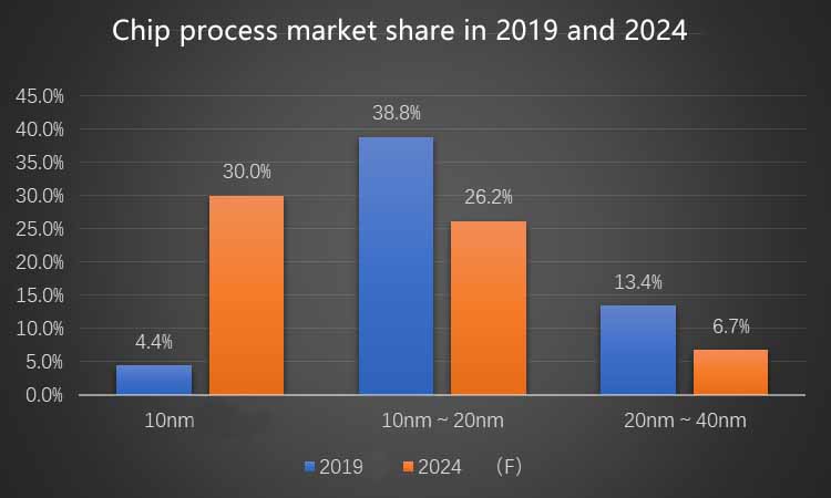
IC Insights data shows that in 2019, the market share of advanced processes below 10nm is only 4.4%, and its proportion will grow to 30% by 2024, while the market share of 10nm to 20nm process will drop from 38.8% to 26.2%, and the market share of 20nm to 40nm process will drop from 13.4% to 6.7%.
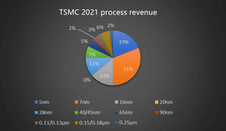
TSMC's 2021 revenue shows that its major revenue lies in advanced processes rather than mature processes, with TSMC's revenue from 7nm and below reaching 50% for the full year 2021. In addition, TSMC said in its press conference that 80% of its capital expenditures will be spent on the research and development of advanced processes such as 3nm, 5nm and 7nm. As one of the only two foundries in the industry that can manufacture advanced processes today, its revenue and capital expenditures can show that the market is only getting hotter and hotter for advanced processes.
In addition, in addition to the typical applications of advanced processes in the traditional sense, such as cell phones and computers, it is not difficult to see advanced processes in some applications that were once dominated by mature processes. For example, some companies are already planning more advanced process chips, such as CorePower Technology, NXP, Qualcomm, Nvidia, etc., have released 7nm, 5nm process chips.
The last battle of silicon chips?
2nm is perhaps the last battle in the field of silicon chips today, but also a key battle. And this battle, with TSMC, Samsung struggling to seek ASML high numerical aperture extreme ultraviolet lithography, also began to gradually fight.
Previously, Victor Moroz, a research expert at Synopsys, said that silicon transistors have limited capabilities, and it is likely that it can only be safely miniaturized to 2nm. In addition, as new materials such as graphene are still in their infancy, it is difficult to replace silicon materials in the semiconductor field in a short time. Therefore, the 2nm chip process as the last battle of silicon chips, almost became the industry consensus.
Therefore, all the world's major chip countries and industry dominators, are secretly fighting to "backwater" on 2nm.
June 17 TSMC held a technical forum, the leading foundry disclosed for the first time, by 2024, TSMC will have ASML's most advanced high-value aperture extreme ultraviolet lithography machine for the production of nanochip transistor (GAAFET) architecture of 2nm chips, is expected to mass production in 2025. It is understood that the high numerical aperture extreme ultraviolet lithography with higher lithography resolution, able to reduce the chip size by 1.7 times, while increasing the density by 2.9 times.
Almost the same time, there are reports that Samsung Electronics from ASML to obtain more than ten EUV lithography machine. And Samsung also said its 2nm chips will be mass-produced in 2025. It is not difficult to see, Samsung is also in 3 years for the mass production of 2nm chips to build up strength.
Although the mass production of 2nm chips will take time, but at this moment, TSMC, Samsung Electronics two chip makers coincidentally seeking the next generation of EUV lithography, also means that as the last battle of silicon chips - 2nm battle has been fought. And who will be the final "winner", it is difficult to predict.
2nm does not represent the entire semiconductor
There is no doubt that the 2nm process has been regarded by leading semiconductor manufacturers as the key to occupy the "high ground" in the market, however, does it mean that with 2nm technology, it has the control of the semiconductor manufacturing industry?
Zhou Peng, vice president of the School of Microelectronics at Fudan University, said that the biggest challenge faced by 3nm, 2nm and even the future 1nm advanced process in the process of advancing may not lie in technology development, but in cost. 28nm node chip design costs only 51.3 million U.S. dollars, while 7nm and 5nm node chip design costs jumped to $297.8 million and $542.2 million, respectively. billion.
The high cost of expenditure, is the major manufacturers have to face the challenge, but the high investment does not mean that the chip can be successfully exchanged for mass production. To photolithography, for example, TSMC and Samsung for mass production of 2nm chips spent a lot of money to buy ASML's high-value aperture extreme ultraviolet lithography, but this does not mean that the possession of the photolithography can rest easy.
Zhou Peng said, the accuracy of the lithography directly determines the accuracy of the chip process, but in the 2nm process technology, high numerical aperture EUV technology, as well as light sources, mask tools and other technologies are in urgent need of optimization. "In addition to the photolithography machine, the deterioration of the interconnect metal resistance, the need for high-precision deposition and etching processes, and the development of three-dimensional integration and packaging technologies for circuits are all technical challenges that must be addressed during the development of the 2nm process." Zhou Peng said.
As can be seen, the process process advancement is also accompanied by a significant increase in costs, resulting in semiconductor manufacturing companies to bring the return on investment ratio may not be as fruitful as imagined. Therefore, it can not be asserted that the mastery of 2nm technology has mastered the semiconductor manufacturing "high power", compared to the advanced process process brings the density, power consumption and other performance advantages, the linear rise in manufacturing costs are more worthy of attention, the future, the need to find a balance between the development and manufacturing of advanced processes and cost expenditures, and this is not an easy task.
Although, in the 2nm "backwater battle", it is difficult to have the final control of the company, and ultimately can stand on the high ground of few companies, but this does not mean that the development of advanced processes and meaningless.
Zhou Peng said: "Moore's law of each process node breakthrough, for the development of the integrated circuit industry has extraordinary significance, but also will inevitably change the entire semiconductor industry market pattern, therefore, advanced process node research for foundry manufacturers and the development of the entire semiconductor industry is crucial. No matter who the future leader in the field of advanced processes is, the ultimate beneficiaries will be the entire IC industry and everyone who enjoys high performance electronic products."

Phone:+86-137-5112-7429
Email:sales@hyx-tech.com
Address:14D2, block A, Modern window building,ZhenHua Road,Futian District, Shenzhen
 sales@hyx-tech.com
 +86-0755-2399-7487
 sales@hyx-tech.com
 Login
Login Register