Date:2022-12-31 14:47:39 Views:1058
Japan's Rapidus and IBM announced on Dec. 13 this year that they have established a partnership for the mass production of 2nm logic semiconductors.
IBM has been actively developing cutting-edge semiconductors for many years and used to have its own 300mm wafer fab in New York State, USA (transferred to Global Foundries in 2014, which was later acquired by ON Semiconductor). In addition, IBM is also producing the required semiconductors for its own branded computers, as well as providing cutting-edge process technology development services and wafer foundry services to its customers.
IBM's cutting-edge process technology development services serve as a Common Platform to reduce R&D costs and secure second-supplier resources by creating common process technologies and production lines. Initially, IBM, Chartered Semiconductor Manufacturing (now Global Foundries), and Samsung Electronics each provided common R&D processes in their respective factories to develop 90nm processes (and more advanced ones). Later, Infineon and Freescale Semiconductor (now NXP Semiconductors) also participated in the development of the 32nm process. In addition, IBM joined Sony and Toshiba to develop and produce the "Cell" for PLAYSTATION 3, and later, collaborated with AMD to develop SOI-related technologies. In the last year (2021), it was reported that Intel was working with IBM on cutting-edge semiconductor research and development. In summary, IBM has experience with most semiconductor manufacturers.
Research and development and mass production are "two different things"
In the case of the previous Common Platform, it was in fact a "Copy Exactly", i.e. an exact replica of the process built on the IBM production line and applied to other "partner factories". Therefore, from the initial stage to obtain a very high yield.
However, according to my understanding, even with the same equipment, the same process, and the same equipment parameters, the same yield may not be obtained. When IBM, Toshiba and Sony produced Cell processors in their respective semiconductor factories, it was said that only IBM had the lowest yield. It can only be said that Japan at that time was still producing cutting-edge logic semiconductors, so it had the appropriate mass production technology.
As mentioned above, after 2014, IBM began to gradually abandon its mass production lines, with the company retaining only its R&D group for cutting-edge processes. We can see from the words of Mr. Dario Gil, IBM's senior vice president and director of IBM Research, in an interview: "The trend of semiconductor development is innovation, which must be achieved through research and development". Moore's Law has always been supported to today is the process of miniaturization. That is, only a more subtle process can help carry more transistors, while the richer the performance of a single chip. Ultimately, the higher the added value of the end product, and it becomes a source of growth for the company's performance. In recent years, companies such as Google and Microsoft are competing to design their own LSI/SOC, that is, according to their own needs to design and produce special LSI, and then provide customers with special services, this practice is the Japanese OA (Office Automation, Office Automation) equipment companies have always been the "play". For several years, it has not changed.
Why did Rapidus introduce IBM's 2nm process?
After the partnership is established, Rapidus will send technical staff to IBM's Albany Nano Tech Complex in Albany, New York, USA (IBM's primary location for advancing R&D) to learn the process. Rapidus is also working with companies outside of IBM to develop 2nm processes with the goal of starting volume production by the latter half of the 2020s (2026-2029).
Rapidus is actively building a system for developing cutting-edge semiconductors and, like IBM, has established a partnership with imec, a European research center specializing in developing cutting-edge semiconductor processes.

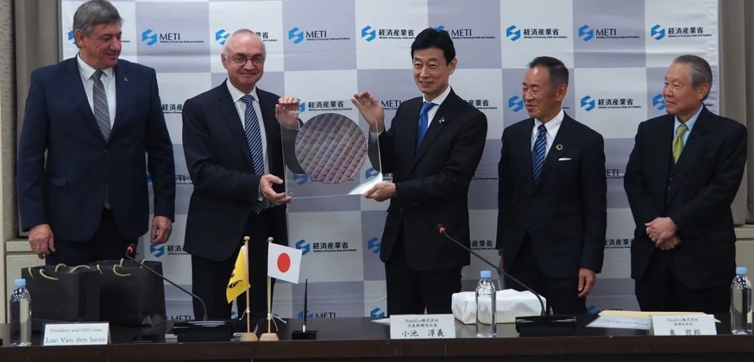
Rapidus and imec sign a Memorandum of Cooperation (MOC)
(Image from: Ministry of Economy, Trade and Industry of Japan website)
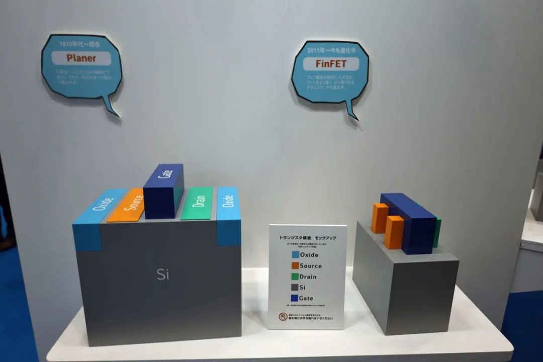
However, the concern is whether the 2nm process will be successfully introduced in the second half of the 2020s. Since this is a mass production project developed from scratch and not a step-by-step process along the line of miniaturization, objectively speaking, it will still take some time. This time, IBM and Rapidus are working directly from Planer to FinFET type. Even a direct challenge to the GAA type is very difficult (not to mention that this time Rapidus avoided the GAA type), in this regard, Rapidus's Junyi Koike, on behalf of the Board President, said: "From FinFET to Nano-sheet is a huge jump. It is difficult to get the GAA technology essentials if you have not been working on cutting-edge process development for a long time. Because of the change in structure, it will be beneficial to make the jump after learning at Albany".
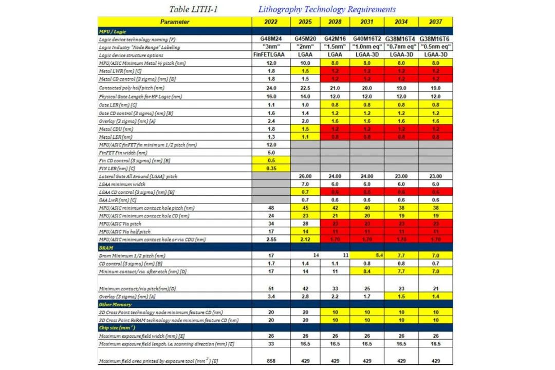
Also at the press conference, Mr. Koike noted, "Although it is a big challenge, it is not impossible to surpass it." Although GAA can adopt most of FinFET's processes, it is also difficult to learn. In addition, from the IRDS 2022 disclosure of logic semiconductor manufacturers boast "nanometer process technology blueprint", 2nm process mass production in 2025. 1.5nm process mass production in 2028 and 1.0nm mass production in 2031, even if Rapidus and IBM succeed in the second half of the 2020s (Even if Rapidus and IBM succeed in mass production of 2nm in the second half of the 2020s (2026-2029), their processes are likely to be 1 or 2 generations behind other advanced manufacturers.

IRDS 2022 lithography blueprint.
(Image from: IEEE IRDS website)

Transistor shape model displayed at the SEAJ booth at SEMICON Japan 2022.
On the other hand, it can be seen that IBM has two main objectives.
First, to find and secure a corporate partner to collaborate on the development of cutting-edge processes.
Second, to add a Foundry company that can actually produce and manufacture wafers.
It is well known that IBM does not have a Foundry factory, and Samsung Electronics has long been OEM for IBM for cutting-edge logic semiconductors. According to foreign media reports, the yield of the most advanced 3nm process is very low and difficult to improve (in addition, there is also information that the yield of 5nm has only recently improved to 70%). The above information may be hearsay, but TSMC is also said to have struggled with 3nm volume production, so it will take a long time to mass produce cutting-edge processes with high yields. For IBM, it is important to find a Foundry mass production manufacturer other than Samsung Electronics.
In fact, at the opening ceremony of SEMICON Japan 2022 (i.e., the discussion session), Mr. Koike pointed out that "Japan is 10 to 20 years behind in cutting-edge logic semiconductors, and it would be very beneficial if we could get technical support from IBM. At a press conference on December 13, 2022, the chairman of the board of directors of Rapidus, Tetsuro Higashi, said, "A Japan-U.S. cooperation project like today's was proposed by IBM two years ago.
In this sense, Rapidus wants to grasp the technology of cutting-edge process as soon as possible, and IBM wants to find a second Foundry manufacturer, so it can be said that the two "hit it off"!
The biggest problem of mass production: procurement of EUV lithography, technology maturity
Even if Rapidus learned IBM's 2nm process technology in Albany, it may not be able to directly mass production.
The biggest problem is not IBM, but the EUV exposure equipment installed in SUNY Polytechnic Institute (including Albany Nano Tech Complex): ADT (Alpha Demo Tool, the first generation of EUV trial equipment), the third generation of "NEX:3300B". (At least IBM has not announced the introduction of new EUV exposure equipment other than the above two devices)
On the other hand, it is necessary to be proficient in the use of the world's latest EUV equipment in order to be able to mass produce 2nm processes (and more advanced processes) and to achieve Mr. Koike's goal of "becoming the world's shortest delivery company".
In addition, it is predicted that TSMC should not use the new generation, high NA EUV (here, NA = 0.55). If, however, there is a technology gap between the EUVs available to IBM and those needed for actual mass production, it will be necessary to fill that gap.
On the other hand, imec, the world's most advanced R&D unit for cutting-edge technologies, has also established a partnership with Rapidus. It is said that imec has also established a partnership with ASML and is introducing ASML's latest EUV exposure machine for its R&D work. Rapidus should be able to use its partnership with imec to acquire the technology related to ASML's latest generation lithography machine and fill the above gap.
However, another issue is whether Rapidus will have access to lithography machines. ASML's 2022 lithography machine shipment forecast is 55 units. 60+ units in 2023 and 90 units planned for 2025. Although ASML is gradually increasing production capacity, but with the development of semiconductor process miniaturization, the number of layers using EUV will also increase, therefore, the future of semiconductor manufacturers will continue to "compete" for lithography machines. It is said that due to the difficulty of purchasing lithography, Samsung Electronics leaders went to ASML in the fall of 2020 after negotiations, and successfully introduced 15 units in 2021.
With the launch of the company, the Japanese government deployed 70 billion yen (about 3.5 billion yuan) from the national treasury to support Rapidus, which is said to be planned to be used for the company's basic operations, but in fact, the funds can be implemented only after a period of time. Even if mass production is achieved, a certain number of lithography machines will be needed. In this sense, it is still uncertain whether mass production will be achieved in the second half of 2020, given the schedule for building factories and introducing equipment.
What will be produced using the 2nm process?
After Rapidus disclosed its goal of mass production of 2nm, many voices pointed out, "What will be produced using the 2nm process?"
Companies such as Toyota, Denso, NTT, and IBM have invested in Rapidus, and it is assumed that all of these companies want Rapidus to OEM semiconductors for them. But what's more important now is whether Rapidus can get cutting-edge Fabless customers like Apple, Qualcomm, AMD, Nvidia and MediaTek. All of these customers are currently commissioning TSMC and Samsung Electronics to produce their semiconductors. The aforementioned customers who need to adopt cutting-edge processes fully understand the added value of cutting-edge processes, which will not change much even in the 2nm era.
Here is a discussion topic that is more similar to process miniaturization: What is stored after increasing storage capacity? Each time there will be a new way of applying NAND (and occasionally a price dip). The need for higher speed and lower power consumption to handle the huge amount of data to be born in the future, in addition to the performance required by super computers (Super Computer) is not yet clear. Because of the increased computing power, real-time (Real Time) AI processing is achieved, and the complex, long-time motion of molecules can be simulated. From the historical experience, some company must find a new use and use it as a new business opportunity and establish a market. Even if it is 2nm, it will follow the above pattern. Therefore, it is important to master the semiconductor performance technology required by the user company.
In addition, to give birth to the above-mentioned new market, it is necessary not only to foster Fabless semiconductor manufacturers, but also to prepare the design and R&D environment of the industry. According to the previous IDM (Integrated Design and Manufacture) model, a company designs and produces semiconductors, and the fab only needs to produce semiconductors for the parent company, and the parent company specifies the function of the semiconductor, and the needs are very clear. However, in today's era of clear division of labor between Foundry and Fabless, it is not meaningful to have production capacity alone, it is more important to provide higher value products to customers based on their own capabilities. Even if you have a high level of technology, you can't generate a deal without customer approval.
For Rapidus' business, Mr. Koike listed three points: first, human resource development; second, building a production system based on end markets and products; and third, green transformation (GX) based on semiconductors. It is indeed very difficult to start developing cutting-edge semiconductors now and then catch up with advanced manufacturers within a certain period of time. Mr. Koike and Mr. Tetsuro Azuma, who have been active in the semiconductor industry for a long time, should be fully aware of this. Mr. Koike has accumulated production experience since the days of Trecenti Technology (the Foundry plant established by Hitachi, Ltd. and UMC, and now the N3 line of Renesas Electronics' Naka plant), and he still has a high level of enthusiasm for Foundry construction. In this sense, Rapidus is expected to develop a mass production process and overcome the above-mentioned difficulties under Mr. Koike's leadership. Can cutting-edge logic semiconductors really be produced on Japanese soil again? Let's keep an eye on the future of Rapidus, which is taking the first step toward this goal.