Date:2022-11-16 11:13:53 Views:837
Introduction
Imprint lithography is a well-known and effective technique for replicating nanoscale features. Nanoimprint lithography (NIL) fabrication equipment employs a stencil technique that involves the field-by-field deposition and exposure of a low-viscosity resist deposited on a substrate by a jetting technique. A patterned mask is placed into the liquid, and the liquid then flows rapidly into the relief pattern in the mask by capillary action. After this filling step, the resist is cross-linked under UV radiation and the mask is then removed, leaving the patterned resist on the substrate. This technique realistically reproduces a higher resolution and greater uniformity than the patterns produced by photolithography equipment. In addition, because this technique does not require the wide diameter lens arrays and expensive light sources required for advanced lithography equipment, NIL devices achieve a simpler, more compact design that allows multiple cells to be clustered together for increased productivity.
Previous studies have shown null resolution better than 10 nm, making the technology suitable for printing several generations of critical memory levels with a single mask. In addition, resistors are used only where necessary, thus eliminating material waste. Considering the absence of complex optics in the imprinting system, the reduction in tooling costs when combined with simple single-level processing and zero waste leads to a cost model that is very attractive for semiconductor storage applications.
Any new lithography technology to be introduced into manufacturing must have a performance advantage or cost advantage. Key technical attributes include alignment, coverage and throughput. Coverage and throughput results for test wafers have been reported in previous papers.In 2018, Hiura et al. reported mixed matched overlay (MMO) at 3.4 nm and single machine overlay (SMO) at 2.5 nm using the FPA-1200 NZ2C four-station cluster tool. These results were achieved by combining an amplified actuator system with a high-order distortion correction (HODC) system, resulting in high-order distortion term correction up to K30.
In this review paper, we touch on the markets that can be processed with zero data and describe efforts to further improve the performance of zero data processing. In addition, we describe recent efforts to develop a pattern transfer process for resolving edge placement errors.
Finally, we describe Canon's efforts to develop a sustainable future and how new methods can be applied to reduce waste and achieve environmentally friendly solutions.
Applications and Markets for Nanoimprint Lithography (NIL)
Unlike other die-making methods for semiconductor devices, NIL has the potential to impact other markets, as shown in Figure 1. In addition to storage and logic, the device space covered includes CMOS image sensors, diffractive optical elements, and meta-optical elements (MOEs). This paper discusses dynamic random memory (DRAM), logic (logic), and meta-optical elements (MOEs). This section of the paper also includes an update on how to address defects and how machine learning can drive NIL performance.
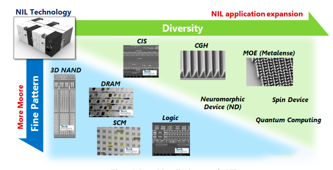
Figure 1. The potential application space of NIL.
a.DRAM
Recent work has focused on developing NIL for advanced memory applications such as DRAM and storage-like memory. DRAM memory is challenging because the DRAM development roadmap requires continuous scaling to eventually reach 14nm or even higher half-pitch (pitches). For DRAM, the coverage on certain critical layers is much tighter than NAND Flash, with an error budget of 15-20% of the minimum half-pitch. For 14nm, this means 2.1-2.8nm. The device roadmap, which includes DRAM overlay requirements is shown in Figure 2. DRAM device design is also challenging, and layout does not always favor pitch division methods like SADP and SAQP. This makes direct printing processes such as NIL an attractive solution.
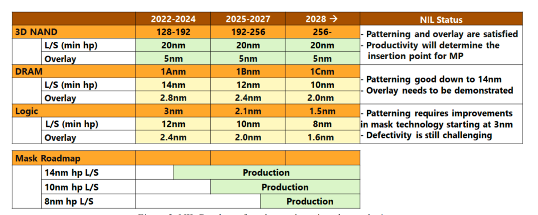
Figure 2. NIL Roadmap for advanced semiconductor devices
In recent years, in order to produce high-volume devices, device manufacturers need to consider more than just coverage error; a few years ago, the concept of edge placement error was introduced. Edge placement error (EPE) is the difference between the expected features of the circuit layout and the printed features. For example, consider a line in a device that must be placed precisely so that the contacts fall correctly on that line. Deviations or errors result in misalignment, which in turn affects the yield of the device. Although conceptually simple, the number of EPE contributors increases significantly due to the need for complex multi-mode schemes. Figure 3a shows a simple example of EPE for a single line and through-hole.Mulkens et al. presented EPE budgets for the case where both ArF immersion and EUV exposure are required (Figure 3b) [11,12].EPE budgets are classified into four categories: optical proximity correction (OPC), coverage accuracy, GCDU, and LCDU.Each classification has a different budget except for OPC Except for OPC, each classification has a different budget. For example, LCDU includes source and mask optimization, scanner optics and dynamics, and resistance and process control.
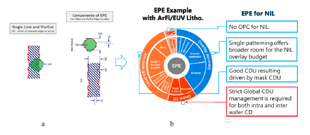
Figure 3. a) Schematic of EPE for line and via b) Breakdown of EPE budget
For NIL, using a single exposure step, the terminology becomes more simplified as follows:
OPC terms:No OPC required
Overlay accuracy:Single pattern application provides more budget for no overlap
LCDU: Good local CDU driven by imprinted mask CDU and reduced linewidth roughness
GCDU:Strict GCDU requires intra- and inter-wafer CD
Based on this model, the total NIL EPE for the DRAM active layer (AA) to storage node contact point (SNC) case can be expressed as:

To solve the EPE problem, the NIL must reduce the coverage error and develop mode transfer methods to minimize the linewidth roughness and optimize the critical size uniformity.
To solve the coverage problem in nanoimprinting systems, there are many factors to consider, some of which are very different from those required by lithography tools. In photolithography, high-order compensation is achieved by manipulating the lens and sensing stage during exposure. Nanoimprinting requires a different approach. A combination of two techniques can achieve high-order distortion correction for null values.
One is the use of a discharge actuator, which applies force through a set of piezoelectric actuators.
The second is a thermal input, which is provided by a DMD to correct the distortion of one field after another.
HODC methods have been proposed in the past, and recently additional correction methods have been applied to drive cross-matching machine overlays (XMMO) to ArF immersion scanners down to 2 nm. other terms include:
Drop mode compensation
Impression force
Impression tip/skew control
Fine Masking
Circular area chuck pneumatic
Details on these calibration methods can be found in References 14 - 16. Figure 4 illustrates graphically the various tuning knobs used for NIL.

Figure 4. To solve the coverage problem, many factors need to be considered. In general, the process can be divided into two categories:alignment and distortion.
In Figure 5, we show the latest XMMO results. the NIL is matched to an ArF immersion lithograph and the reported results show measurements for all electric fields with 322 positions per field. The full-field XMMO is on the order of 2 nm mean + 3 σ, with slightly higher results for the full and partial electric fields, with x and y values of 2.30 nm and 2.21 nm, respectively. recent improvements have focused on the partial electric fields, including methods designed to improve the coverage convergence time, as shown in Figure 6.
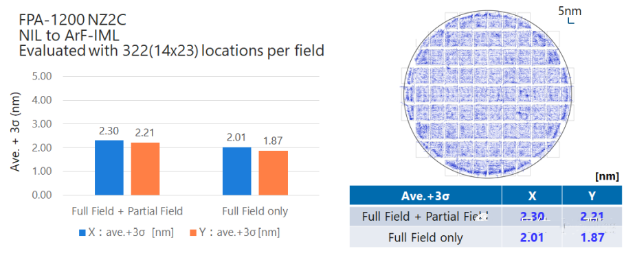
Figure 5. Cross-matching superposition of full and local electric field NIL values
In this example, control points or points of interest for alignment are placed at the center of the TTM markers, thereby accelerating alignment convergence and reducing overlap errors in part of the electric field. In this example, the alignment error in the Y direction is reduced from 2.20 nm to 1.79 nm at 3σ, while other methods under development include a new final impression force and tilt control system that allows more precise control of impression force and tilt.
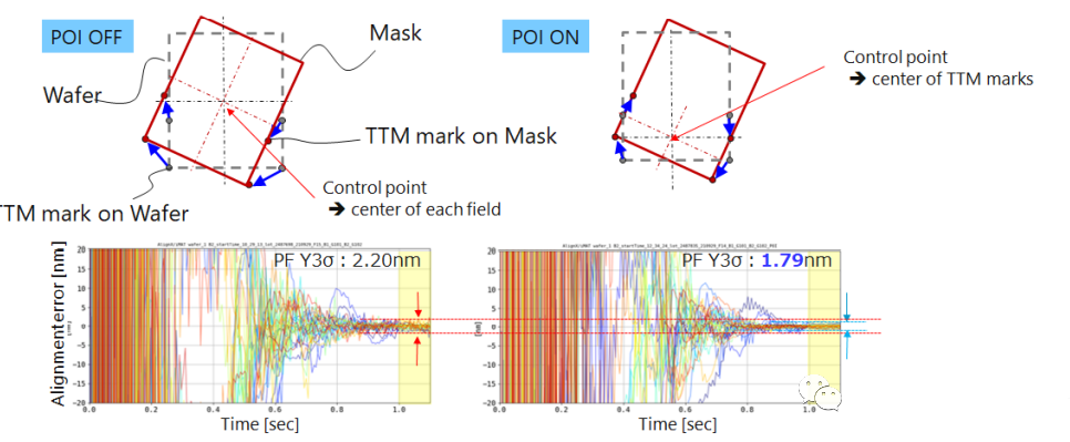
Figure 6. Alignment control point (POI) impact
The NIL pattern transfer process consists of three separate etching steps, starting with resist stripping (residual layer etching), followed by etching of SiARC and spin-coated carbon film (Figure 7). In TEL's preliminary study, the quasi-atomic layer etching process developed by TEL was applied to the SiARC layer. The q-ALE process is depicted in the figure on the right, where layer-by-layer etching is achieved through fluorocarbon adsorption and alternating bombardment with Ar ions.
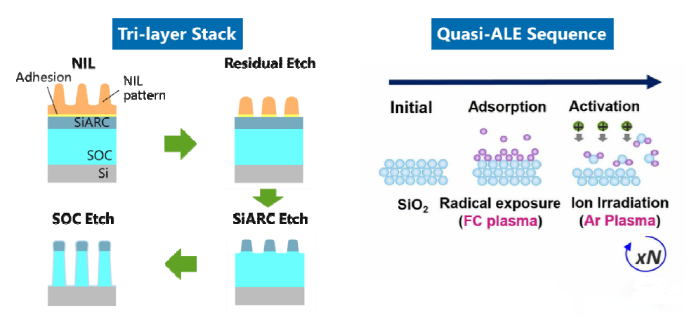
Figure 7: Pattern transfer techniques are critical and the integrated solution needs to meet critical dimensional uniformity specifications. As with other advanced lithography methods, NIL uses three layers of resist.
Results of the first etch study show 19nm and 32nm half-pitch lines and pitches (Figure 8).
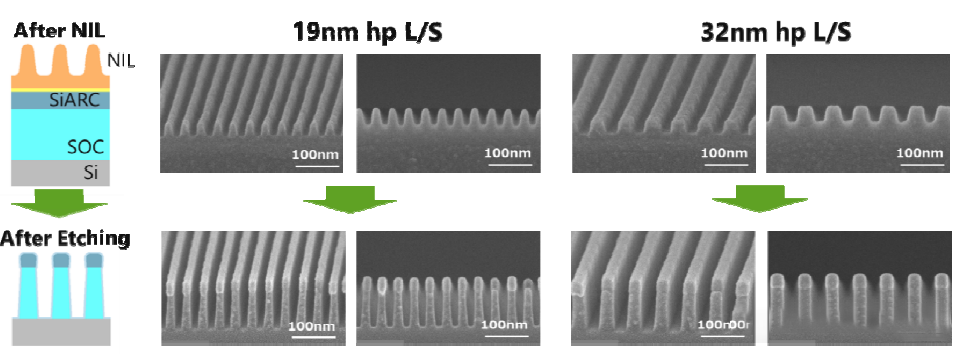
Figure 8. Patterned transfer of 19nm and 32nm half-pitch lines using a three-step etch process. The process uses the aquasi-ALD method developed by TEL.
For NIL, it is possible to adjust the CD after etching by changing the residual layer thickness (RLT) on the wafer, and it is also possible to adjust the final CD after etching because the volume of resist injected within a field and from one field to another can be precisely controlled by the accuracy of the picoliter, so that the above process can be achieved. In general, thinner RLTs lead to smaller critical dimensions after etching, as shown in Figure 9a. The correction amount is a function of the etching process, and three examples are shown in Figure 9b. Note that the slope changes as the etch conditions change, so adjustments of the order of 1 to 3 nm can be made.
The pattern transfer process can also be used to manage line width roughness (LWR), an example of which is shown in Figure 9. After NIL exposure and pattern transfer to a 19 nm half-pitch feature, the LWR was measured using a Hitachi CG6300 scanning electron microscope, and the feature image and resulting unbiased LWR are shown in Figure 10. Note that the LWR was reduced to 2.6 nm after pattern transfer, and this type of reduction can also be observed in other LWR studies. Finally, we note that CD can also be adjusted to a lesser extent depending on the NIL exposure dose. Interested readers are referred to the paper on edge placement errors in this proceedings by Ogusu et al.
b. Logic
The second market of interest is in the area of logic. 2021, Canon, together with other major Japanese semiconductor manufacturing equipment companies, has applied for the "Post-SG Information and Communication System Enhancement Infrastructure" R&D project initiated by the New Energy and Industrial Technology Development Organization (NEDO) for the expansion of logic devices. miniaturization. The program has been approved on the subject of scaling logic devices beyond the 2nm node. A schematic of the NEDO project organization is shown in Figure 11.
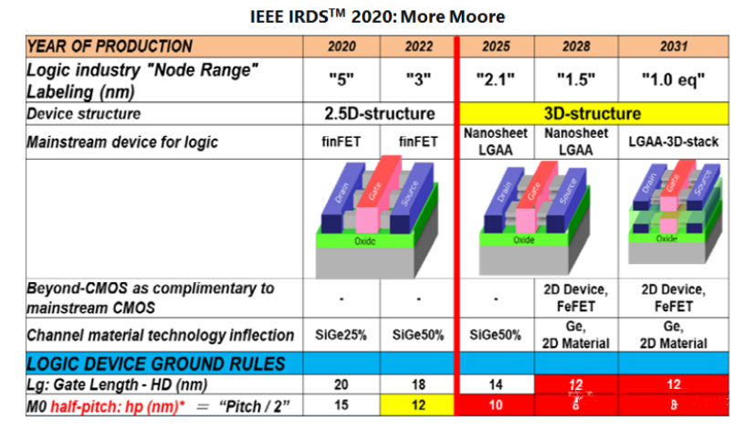
Fig. 12. Development targets for nano-sheet devices
c. Optical Elements (MOEs)
Optical elements (MOEs) are patterned hypersurfaces with potential uses as optical elements used in cameras, cell phones, and other devices that rely on concentrating lenses to form images. With the introduction of hypersurfaces, it is expected to shrink lenses and eliminate past limitations. A hypersurface typically refers to a two-dimensional counterpart of a metamaterial, either structured or unstructured, with subwavelength-level patterns in the horizontal dimension.
Because metasurfaces are planar structures with ultra-thin characteristics, they do not produce chromatic aberrations - they are "achromatic lenses" - because all wavelengths of light pass through them almost simultaneously. They also have the advantage of tunable dispersion - the ability to control how the color of light is dispersed compared to glass or other conventional materials with fixed dispersion. Wavelengths of interest include the infrared and UV/Vis spectra.
In the example shown at right, note the variation in the size and direction of the elemental features. Early work on optical elements relied heavily on electron beam writing, which, while attractive for prototyping, is not applicable to production. nIL is a strong option for patterning the production of optical elements because there are few patterning limitations associated with the technology.
d. Defect Management
A common theme across all devices is defect and defect management. Each device type has its own requirements, which dictate strategies and practices for managing the various sources of defects. Logic devices have the most stringent requirements, while DRAM tends to be more lenient compared to logic. Metal oxide semiconductors are more of an average device and the level of defects required is not as stringent as for the most advanced semiconductor circuits.
Several papers have been published on methods to reduce the source of zero defects. Recent work looks at in-situ particle cleaning and particle detection. The wafer particle detection (WPC) system has a sensitivity of about 200 nm for blank wafers and has been confirmed by comparison with the KLA-Tengco SP3 tool, as shown in Figure 14. This tool will be used as a means to avoid obtaining any duplicate defects on replica masks.
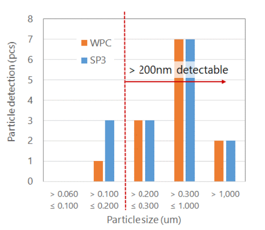
Figure 14: Wafer Particle Inspection (WPC) system sensitivity
e. Artificial intelligence and machine learning for NIL
Finally, Canon is applying machine learning and AI technologies to further improve system performance, increase productivity, and enable more autonomous control to enable rapid system upgrades. The system software is called "Lithography Plus" or Liplus, and Figure 15 shows an example of how this is being applied to NIL. Other areas where Liplus can be applied include alignment optimization, anti-jet and vibration reduction.
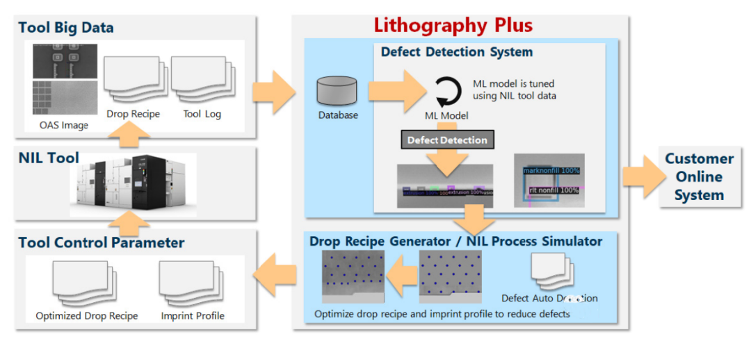
Figure 15: Liplus enables rapid optimization of NIL processes and performance. In this example, a machine learning algorithm is used to detect drop recipe defects and then quickly generate optimized recipes.
3 Sustainability Goals
Finally, we will discuss how Canon is working to develop sustainability and address global issues for the betterment of humanity. This leads to the "list of goals shown in Figure 16", which contains topics such as affordable and clean energy, responsible consumption and production, and innovation and industrial infrastructure.

Figure 16: Sustainable Development Goals
These guiding principles apply to NIL technology, as shown in Figure 17. NIL tools are developed to minimize power consumption and prevent waste. Resist use is minimized by spraying resist directly onto the stepper area on the wafer in a volume comparable to that required to fill the embossed image on the embossing mask, with a thin residual base layer directly below the formed resist pattern.
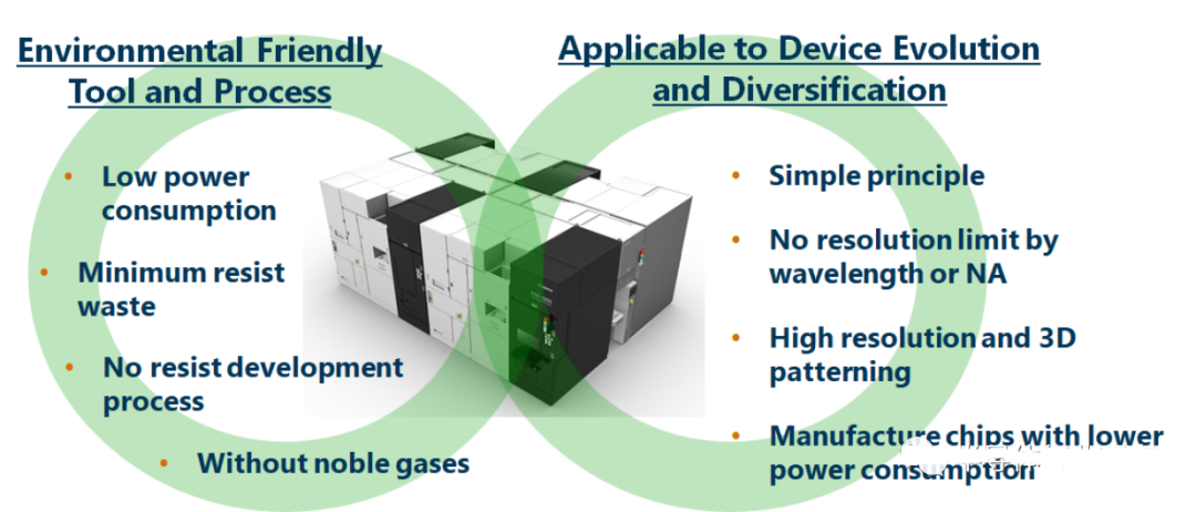
Figure 17: NIL tools and processes are designed to be more environmentally friendly and able to address a more diverse application space
In terms of power consumption, NIL utilizes a simple single-step mode process combined with a lower power exposure source to reduce power consumption, regardless of the device node as shown in Figures 18a and 18b.
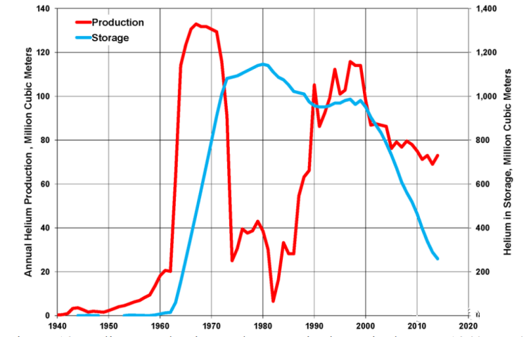
Figure 18: Comparison of power consumption for a) BEOL fabrication and b) full chip fabrication.
As a final example, we consider the resist filling process after jetting, which requires the removal of any gas present to complete the droplet coalescence and feature filling steps. Helium has been used because it diffuses readily into fused silica masks. However, the world is currently facing a shortage of helium. As an example, Figure 19 shows U.S. production and storage for the past 70 years, with recent trends evident for both.

Helium production and storage in the United States from 1940-2014 shown in Figure 19
To counter this trend, we have recently looked at alternative gases such as nitrogen and helium. Gas permeability is essentially the product of the solubility coefficient and the diffusion coefficient. With the right material, it is possible to remove CO2 more efficiently. as shown in Figure 20, where the resistive fill time is modeled as a function of the spin thickness on the underlying carbon (SOC) film. To achieve faster filling, a minimum SOC thickness is required. Further experimental studies are needed to understand this mechanism, but a roadmap is now in place to reduce or eliminate the use of helium.
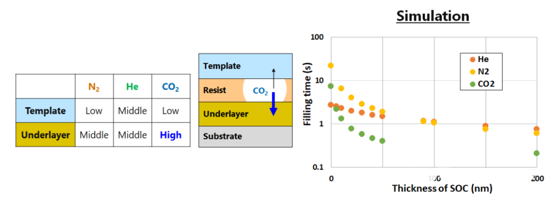
Figure 20: Simulation of the block filling time as a function of spin on carbon thickness for three different gases:helium, nitrogen and carbon dioxide. In the presence of a thin carbon layer, CO2 is observed to outperform the helium baseline process.
4 Conclusion
Imprinted lithography is a well-known and effective technique for replicating nanoscale features. Nanoimprint (NIL) fabrication devices employ a stencil technique that involves field-by-field deposition and exposure of a low-viscosity resist deposited on the substrate by jetting techniques.
Previous studies have shown that the null resolution is better than 10 nm, making the technique suitable for printing several generations of critical memory levels with a single mask. In addition, resist is used only where necessary, thus eliminating material waste. Considering the absence of complex optics in the imprinted system, the reduction in tooling cost when combined with simple single-level processing and zero waste leads to a cost model that is very attractive for semiconductor storage applications.
In this review paper, we have touched on markets that can be addressed, including advanced memory, logic and meta-optics. We also describe efforts to further improve NIL performance, including defect mitigation and machine learning algorithms. In addition, we report on recent efforts to develop a pattern transfer process that can be used to address edge placement errors by adjusting critical dimensions of wafers and reducing line edge roughness.
Finally, we discuss Canon's efforts to develop a sustainable future and how new methods can be applied to reduce waste and achieve environmentally friendly solutions.
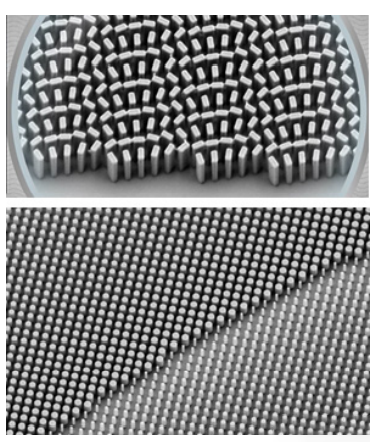
Figure 13: Example of a super-optical element. MOE patterns can be configured to operate in the IR or UV/Vis spectrum.