Date:2022-10-19 10:40:13 Views:1005
TSMC engineers, in collaboration with two universities in Taiwan, will report at this year's International Electron Devices Meeting (IEDM) on the world's first nanosheet gate ring transistor made from a two-dimensional semiconductor material.
The silicon nanosheet transistor or aka nanoribbon offers improved electrostatic control and relatively high drive current and is implemented in a 3nm manufacturing process.
According to the highlights of the upcoming IEDM program, TSMC has demonstrated the possibility of using transition metal disulfide monolayers as semiconductor channels in nanosheet transistors. In this case, it is molybdenum disulfide.
This two-dimensional material can have enhanced electron mobility compared to silicon and spin-orbit coupling, thus yielding the possibility of spintronic computing.
Transistors with a gate width of 40 nm produce a drive current of 410 microamps per micron at a Vds of 1V. The expectation is to increase the drive current by stacking the devices.
The TSMC-led team will report on the integration flow for fabricating such transistors, but optimization of performance remains to be done.
TSMC Paper #34.5 first demonstration of the GAA monolayer MoS2 nanosheet nFET ...... is one of the highlights of the 68th annual IEDM.
In Paper #7.4, near-ideal subthreshold swing in a single-layer MoS2 top-gate nFET with an EOT of 1 nm, a TSMC-led team describes the integration of hafnium-based dielectrics with MoS2 to build top-gate nFETs to create stackable systems. The subthreshold voltage swing is less than 70mV/dec. This indicates a low leakage current when the transistor is turned off.
Major breakthrough in sub-1nm process! TSMC officially announces "bismuth" secret weapon
IBM just announced the development of 2nm chips soon, TSMC again launched a challenge! TSMC achieved a major breakthrough in sub-1nm process, constantly challenging the physical limits. Recently, NTU, TSMC, and MIT collaborated on a study that found that two-dimensional materials combined with "bismuth semi-metal (Bi)" can reach extremely low resistance and approach the quantum limit. The research result, jointly completed by Professor Chih-Yi Wu of the Department of Electrical Engineering and Institute of Photonics at NTU, and a research team from TSMC and MIT, has been published in the international journal Nature, which helps realize the challenge of semiconductor sub-1nm processes.
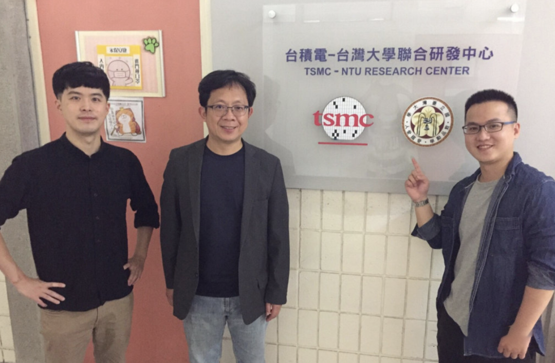
Currently, the mainstream semiconductor process progresses to the 5nm and 3nm nodes. The number of crystals per unit area of the wafer is approaching the physical limit of silicon, the dominant material in semiconductors, and the wafer performance cannot be significantly improved year by year. In recent years, the scientific community has actively searched for 2D materials that can replace silicon to challenge processes below 1nm, but has struggled to solve the problems of high resistance and low current of 2D materials. NTU, TSMC and MIT have launched a 1.5-year-long multinational collaboration since 2019 and finally found this key.
This major breakthrough was first discovered by the MIT team that the electrode with "semi-metallic bismuth (Bi)" on "two-dimensional materials" can significantly reduce the resistance and increase the transmission current. TSMC's technology research department optimized the "bismuth (Bi) deposition process", and finally the NTU team used the "helium ion beam micro shadowing system" to successfully reduce the component channel to nanometer size, finally obtaining a breakthrough research result. Prof. Chih-Yi Wu explained that after using "Bismuth (Bi)" as the key structure of "contact electrode", the performance of two-dimensional material transistors is not only comparable to that of "silicon-based semiconductors", but also has the potential to be compatible with the current mainstream silicon-based process technology, which will help break the limit of "Moore's Law" in the future.
The research results can provide excellent conditions for next-generation chips, such as power saving and high speed, and are expected to be put into emerging technology applications such as artificial intelligence, electric vehicles, and disease prediction in the future.
TSMC is moving towards 2nm!Mass production expected in 2024
For decades, there has been a golden rule behind the progress of the semiconductor industry, namely Moore's Law. Moore's Law states that every 18 to 24 months, the number of components that can be accommodated on an integrated circuit will double, and the performance of the chip will also double.
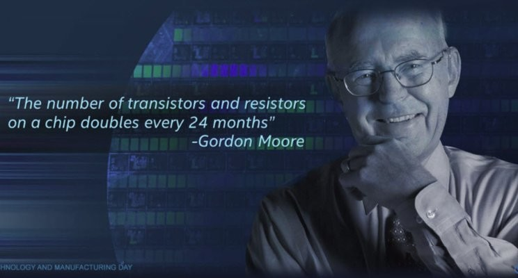
However, in today's Moore's Law slowdown or even failure, the world's major semiconductor companies are still desperately "fighting", hoping to take the lead in the manufacturing process layout of the high point. TSMC is a leader in advanced processes. 3nm, TSMC is the only one in the field. 2020, 5nm mass production. 2nm is expected to be launched in 2023 to 2024. Previous reports have introduced TSMC's entire advanced process layout in recent years.
You know, TSMC, Intel and Samsung are known as the semiconductor manufacturing "Big Three". The three giants are catching up with each other on the way to gradually shrink the chip process.
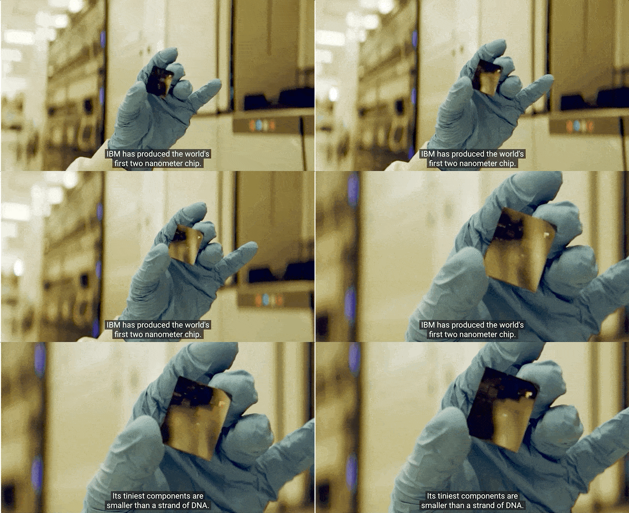
Now halfway there is IBM, last week announced that it has developed the world's first 2nm chip, equivalent to the fingernail size of the chip to accommodate up to 50 billion transistors, faster and more efficient.
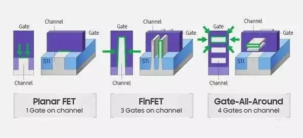
For the more advanced 2nm process, TSMC announced the development of this as early as 2019. Last year, shortly after 5nm volume production, TSMC announced a major breakthrough in the 2nm process - cutting into gate-all-around (GAA) technology. Unlike the 3nm and 5nm FinFET architectures, the FinFET itself has been reduced to its size limit, and the fin distance, short-channel effect, leakage, and material limits have made transistor manufacturing precarious, even when the physical structure cannot be completed.
The fully encircled gate (GAA) is an evolution of FinFET technology, where the channel is composed of nanowires (nanowires) surrounded by gates on all sides, thus again enhancing the gate's control over the channel and effectively reducing leakage. TSMC in the 2nm research and development cut into the full ring gate field effect transistor GAA, its rival Samsung as early as 2 years ago when it revealed its 3nm technology process, announced a shift from FinFET to GAA, and "big talk": 2030 to exceed TSMC, the world's leading chip foundry position.
This is also considered for the two companies 2-3nm process market battle has sounded the horn. In order to complete the development of 3nm before TSMC, Samsung's chip manufacturing process from 5nm directly up to 3nm, 4nm is directly skipped. Although TSMC and Samsung in the 2nm-3nm market you fight, but Intel does not care, still adhere to the 14nm, 10nm process research and development. TSMC, Samsung's pursuit of the most advanced process, precisely want to compete in the world of advanced processes.
TSMC joined the U.S. semiconductor alliance
At the same time, for the benefit of the world's largest foundry, the island company TSMC also actively seeking to build factories in the United States, one of the efforts is to join the recently established "U.S. Semiconductor Alliance. On Tuesday, the Semiconductors in America Coalition (SIAC), a lobbying group led by U.S. technology companies, was formed.
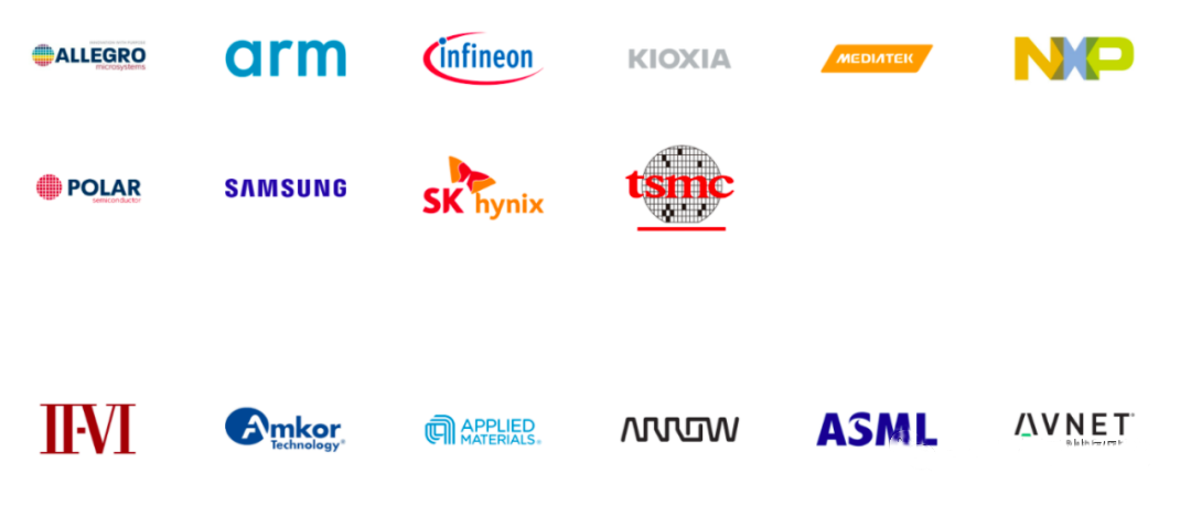
SIAC members currently include Apple, Google, Microsoft and Intel. In addition to these leading U.S. technology companies, they also include Samsung, Hynix, and lithography giant ASML, and even the island's major foundry TSMC and MediaTek. TSMC did not respond specifically to the news of joining SIAC.
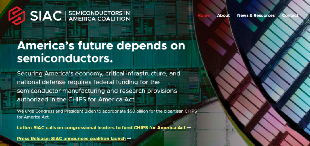
A partial screenshot of the "Members" page of SAIC's official website, where TSMC can be seen listed Restrictions by any of these members could put a damper on our development. SIAC's top priority is to urge the U.S. government to provide "subsidies".
A bipartisan group of U.S. senators on Friday unveiled a "$52 billion" proposal to significantly increase U.S. semiconductor chip production and research over five years. U.S. Senator Mark Kelly and others have been discussing a compromise proposal to "address the rise in Chinese semiconductor production and the impact of chip shortages on auto manufacturing and other U.S. industries. The proposal is expected to be included in a bill to fund basic and advanced U.S. technology research to be discussed in the Senate next week. In addition to this $52 billion proposal, the U.S. Senate Commerce, Science and Transportation Committee voted 24-4 on May 12 local time to pass the "Endless Frontier" bill, which authorizes "$110 billion" over five years for science and technology research, according to The Hill.
The "Endless Frontier" bill would authorize $100 billion over five years to invest in basic and advanced science and technology research, commercialization, education and training programs, including artificial intelligence, semiconductors, quantum computing, advanced communications, biotechnology and advanced energy. In addition, the bill includes an additional "$10 billion" to establish at least 10 regional technology centers and create a supply chain crisis response plan to address issues such as the "semiconductor chip gap" that is affecting automotive production. This makes "mainland China's efforts to upgrade the chip industry, will be more challenging. Capri believes that TSMC's significant increase in investment in the U.S. and its participation in establishing leading 5nm or even 3nm chip manufacturing plants in the U.S. could put pressure on mainland China, as TSMC apparently will not build such plants in the mainland. TSMC confirmed last month that it had invested $2.9 billion to expand its plant in Nanjing, but the technology in that plant is a 28nm process, which is two to three generations behind the technology used by TSMC in its Arizona fab in the United States.
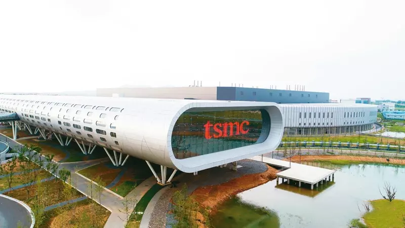
Randall, head of Intralink's electronics and embedded software division, said TSMC, like other companies joining SIAC, was motivated by its own interests and the opportunity to divide up $50 billion in U.S. government funding. At the same time, he said, China does not have a similar organization that brings together companies from around the world, and that teaming up in an alliance would help the United States and its allies "retain a long-term advantage over China.