Date:2022-08-18 17:19:34 Views:1152
With the advent of the era of information and data explosion, the market demand for memory continues to grow. In the finished chip manufacturing segment, the market's reliance on traditional wire bonded packages remains high. There is also a growing demand for the use of multi-chip stacking technology to achieve high storage density in the same size device. Such demand brings not only process capability challenges, but also higher requirements for process control.
As a leading company in semiconductor packaging and testing, what are the innovative practices of Changdian Technology in the field of multi-chip stacking and packaging technology? This article will introduce its technical advantages, process and control capabilities.
Advantages of multi-chip stacked packaging technology
Figure 1 shows the side view of two different types of memory packages. From the package structure, we can see that both packages are made of multiple chips stacked together to reduce the space occupied by the multi-chip package, thus minimizing the size of the memory device. One of the key processes is chip thinning, cutting, and chip lamination.
From the perspective of market demand, flip-chip packaging (FC) and silicon through-hole (TSV), as well as wafer level packaging forms can effectively reduce device size while increasing data transfer speed and reducing the possibility of signal interference. However, in terms of the current consumer market demand, the traditional wire-based packaging forms still account for a large proportion of the advantages of cost competitiveness and technical maturity.
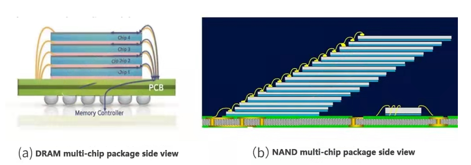
Figure 1 Side view of multi-chip package
The current process capability of Eternal Technology can realize the stacking of 16 layers of chips, the thickness of a single layer of chips is only 35um, and the package thickness is about 1mm.
Key process of multi-chip stacking package chip thinning and cutting
1) Dicing after grinding (DAG)
Mainly for thicker chips (thickness >60um), it is a more traditional packaging process, mature and stable. The wafer is thinned after the protective film is applied, and then the chip is separated by cutting with a blade. It is suitable for most of the packages.
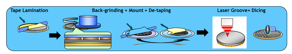
Figure 2 DAG (Source: DISCO)
2) Dicing before grinding (DBG)
Mainly for 38-85um chip thickness and chip circuit layer thickness >7um, for the demand of thinner chips and the increasing number of circuit layers of memory chips (currently the common 3D NAND layer count is 112 layers or more). Using a blade to first half-cut the chip and then thin it, the laser cuts through the die attach film. It is suitable for most NAND chips, and the advantage is that it can solve the problems of side chipping control and die crack in the post-process of ultra-thin chips, which greatly improves the feasibility and mass production of multi-chip packaging.
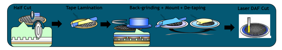
Figure 3 DBG (Source: DISCO)
3) Stealth Dicing before grinding (SDBG)
It is mainly for 35-85um chip thickness and chip circuit layer thickness <7um, mainly for the needs of thinner chips with less circuit layers, such as DRAM, using stealth laser to separate the middle of the chip first, then thinning, and finally chipping the wafer. It is suitable for most DRAM wafers and chips with fewer circuit layers. Compared with DBG, the side chipping control is better because there is no blade cutting mechanical influence. Chip thickness can be further reduced.
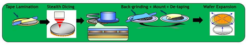
Figure 4 SDBG (Source: DISCO)
Key process of multi-chip stacked package: Chip bonding
(1) Chip position accuracy: Due to the multi-chip stacking, the control of the chip lamination position and the distance between the chip and the chip becomes the key point and difficulty of the process. The introduction of high-precision laminating machine makes ladder-like one-time multi-chip lamination accuracy can be guaranteed at (+/-15um), which can effectively reduce the process yield loss to achieve mass production of multi-chip stacking technology (Figure 5).
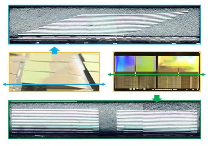
Figure 5: Chip placement in multi-chip stacking
(2) Ultra-thin chip pickup: limited by the chip thickness, using the traditional thimble to peel the chip from the chip carrier film (DAF), the stress is concentrated on the chip of only 1.5 mil (38um), which becomes almost an impossible task. Therefore, specialized jigs were developed for picking up ultra-thin chips. The main function is to peel the chip off the chip carrier film (DAF) by multi-step platform bumping. Compared to conventional ejectors, it spreads the stress from point to surface and changes from one-step ejection to multi-step ejection. It effectively improves the chip concealment cracking problem of ultra-thin chips.
Control of multi-chip stacking process
I. Warpage problem improvement
The thickness of the wafer is getting thinner and thinner after grinding, and the deformation will cause the wafer to be unable to continue the post-process operation, which makes the warpage control of the processed wafer a problem. By SDBG and DBG, and using polishing process at the same time, the wafer surface stress is released and the wafer warpage is improved.
Second, the impact of foreign matter and particulate matter
Although the current cleanroom level has reached 1k (the number of micro-dust is strictly controlled within 1000 per cubic meter), foreign matter and particulate matter in the package shop is a big threat for ultra-thin chips in each process. As shown in Figure 6 below, foreign matter or particulate matter falling on the chip and being squeezed by external force can lead to hidden cracking of the chip.

Figure 6: Problems caused by foreign objects and particles
Therefore, in the critical process (chip-related), the negative pressure equipment HEPA environment is added to avoid foreign objects or particles from falling on the chip surface. For the machine, a cover is added to provide double protection. In addition, we use designated cassettes, carts, and drying cabinets for chip storage and delivery. The frequency of regular cleaning of designated cassettes, carts and drying cabinets can reduce the influence of foreign matter and particles.
As the third largest chip manufacturing company in the world and the first in mainland China, ChangDian Technology has always focused on technology development and innovation as its key development strategy, and has achieved a series of results. With more than 3,200 patented technologies (as of December 31, 2021) and the first prize of the National Science and Technology Progress Award in 2020, ChangDian Technology has always played the role of industry leader and technology leader in the semiconductor industry.
Looking ahead, ChangDian Technology will continue to strengthen innovation, develop finished chip manufacturing technologies including multi-chip stacking and packaging technology, optimize product quality, and continuously improve its technical and service capabilities in the process of the chip industry's continuous development toward leaner development, thereby promoting the development of the entire industry.

Phone:+86-137-5112-7429
Email:sales@hyx-tech.com
Address:14D2, block A, Modern window building,ZhenHua Road,Futian District, Shenzhen
 sales@hyx-tech.com
 +86-0755-2399-7487
 sales@hyx-tech.com
 Login
Login Register