Date:2022-08-01 15:47:52 Views:1267
Integrated circuit (chip) technology has a 64-year history of development since its birth in 1958. In today's information society, the chip is undoubtedly the most important basic support. In recent years, chip core technology has become a powerful tool for the United States to maintain its hegemony in science and technology and to block and suppress other countries. People would like to know how chip technology has developed step by step from its primitive and immature beginning to become the technological jewel in the high-tech crown today. In this article, we will mainly use photos and diagrams, supplemented by text, to talk about the history of the development of chip technology over 60 years. Due to the limitation of space, it is tentatively divided into three articles: the first, the second and the third.
To introduce the history of chip technology, we have to start with the discovery and research of semiconductors, the invention of electron tubes, transistors and integrated circuits. It is because of these discoveries, research and inventions that electronics technology and the electronics industry were born. Since then, human society has opened the prologue of electronic information technology.
1. Semiconductor discovery and research (1833-1947, lasting 114 years)
In 1833, British scientist Michael Faraday Faraday (Michael Faraday) in testing the characteristics of silver sulfide (Ag2S), found that the resistance of silver sulfide with the rise in temperature and reduce the specific phenomenon, known as the resistive effect, which is the first feature of human discovery of semiconductors.
In 1839, the French scientist Edmond Becquerel (Edmond de la Roche) discovered that the resistance of silver sulfide decreased with temperature. Becquerel (Edmond Becquerel) found that the junction formed by the contact between the semiconductor and the electrolyte would produce a voltage under light, which is later known as the photovoltaic effect, referred to as the photovoltaic effect. This was the second characteristic of semiconductors discovered by man.
In 1873, Willoughby Smith of England. In 1873, Willoughby Smith of England discovered the photoconductivity effect of selenium (Se) crystalline materials, which increases the electrical conductivity under light, and this is the third characteristic of semiconductors discovered by man.
In 1874, Ferdinand Braun, a German physicist, discovered the photoconductivity effect of selenium (Se) crystals under light. Ferdinand Braun observed that the conductivity of certain sulfides was related to the direction of the applied electric field. If a positive voltage is applied to its ends, it is conductive; if the voltage polarity is reversed, it is not conductive, which is the rectification effect of semiconductors, the fourth characteristic of semiconductors discovered by man. In the same year, the German-born British physicist Arthur Schuster, who was born in Germany, discovered the fourth feature of semiconductors. Schuster (Arthur Schuster) also discovered the rectification effect of copper (Cu) and copper oxide (CuO).
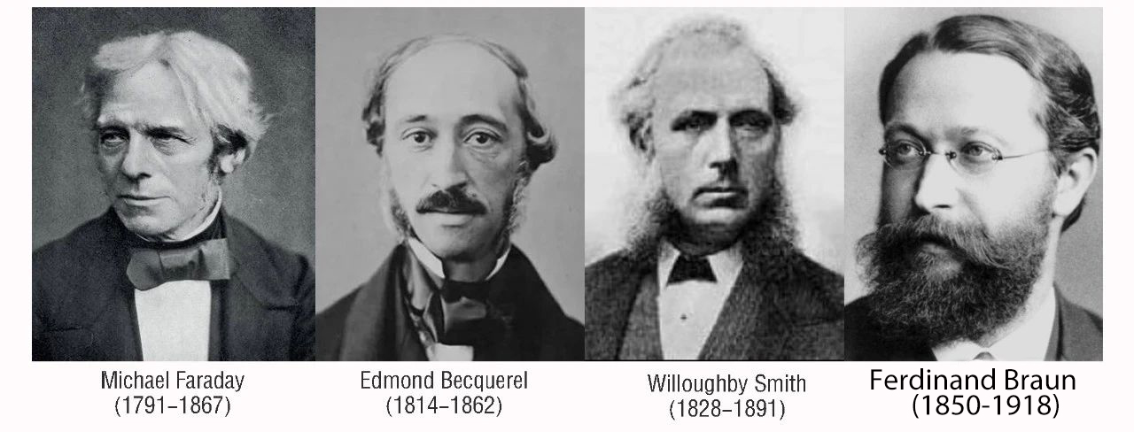
Figure 1. Four scientists who discovered the properties of semiconductors
(Faraday, Becquerel, Smith, Braun)
Although these four effects of semiconductors were successively discovered by scientists before 1880, the term semiconductor was only first used by J. Konigsberger and I. Weiss in about 1911. Later, the rectification theory, energy band theory, and potential barrier theory of semiconductors were only gradually completed through the efforts of many scientists.
In the following two decades, a number of semiconductor applications emerged in the world. For example, from 1907 to 1927, physicists in the United States successfully developed crystal rectifiers, selenium rectifiers and copper oxide (Cu2O) rectifiers, etc. In 1931, selenium photovoltaic cells were successfully developed, and in 1932, Germany successively developed lead sulfide (PbS), lead selenide (PbSe) and lead telluride (PbTe) semiconductor infrared detectors, etc.
In 1947, Bell Laboratories in the United States comprehensively summarized the above four characteristics of semiconductor materials. For 67 years from 1880 to 1947, the research and application of semiconductor materials was very slow because it was difficult to purify semiconductor materials to an ideal degree. Since then, the tetravalent elements germanium (Ge) and silicon (Si) became the semiconductor materials that scientists paid most attention to and researched vigorously. A few years after the invention of germanium crystal triode by W. Shockley, it was found that silicon was more suitable for the production of transistors. Since then, silicon has become the most widely used semiconductor material, and continues to be so today. This is also the reason why Northern California became the center of the silicon industry and was called "Silicon Valley".
Semiconductor materials are materials with conductive properties between conductors and insulators, and their resistance is much greater than that of conductors, but much smaller than that of insulators. Their electrical properties can be artificially modified. Common semiconductor materials are silicon (Si), germanium (Ge), gallium arsenide (GaAs), silicon carbide (SiC), gallium nitride (GaN) and so on.
2. The invention of electron tube (1906, 115 years ago)
In 1904, the British physicist John Ambrose. Ambrose Fleming Fleming (John Ambrose Fleming) invented the world's first electron tube, which is a vacuum diode, and he was granted a patent for this invention.
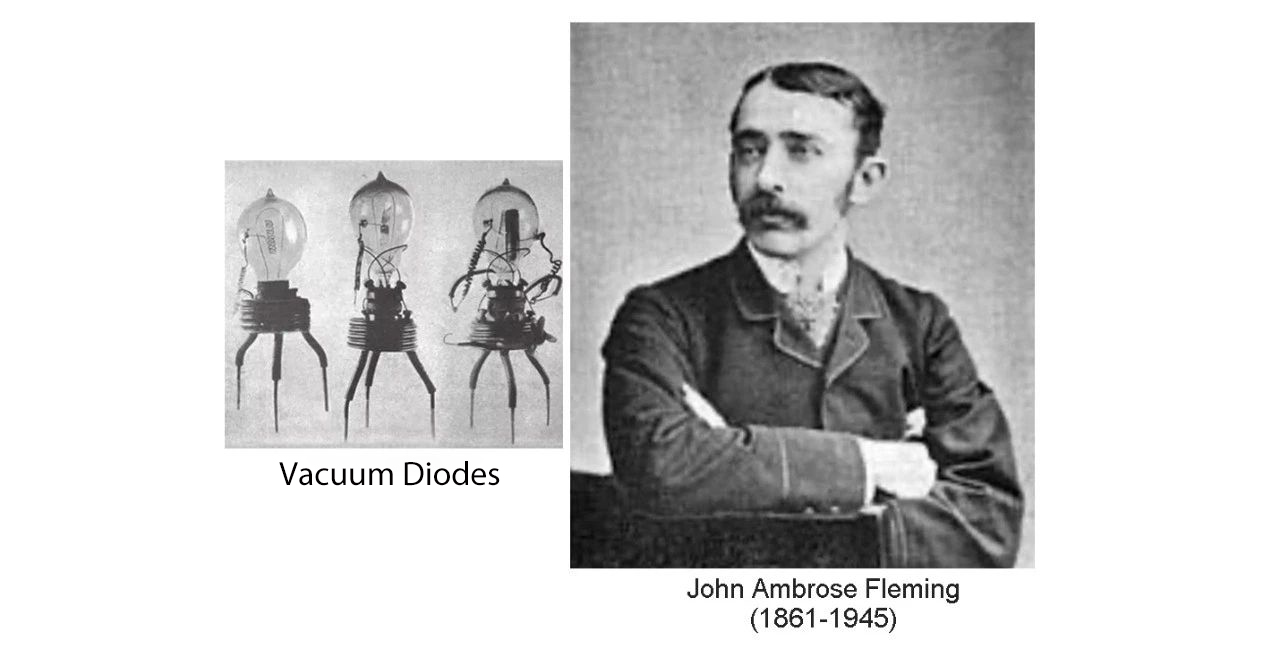
Figure 2. The vacuum diode invented by Fleming
In 1906, the American engineer Lee D. De. Forrest (Lee de Forest) in Fleming vacuum diode based on the addition of an additional grid, invented another tube, it is a vacuum triode, so that the tube in addition to the detector and rectification function, but also has the function of amplification and oscillation. Forrester got the patent for this invention on February 18, 1908.
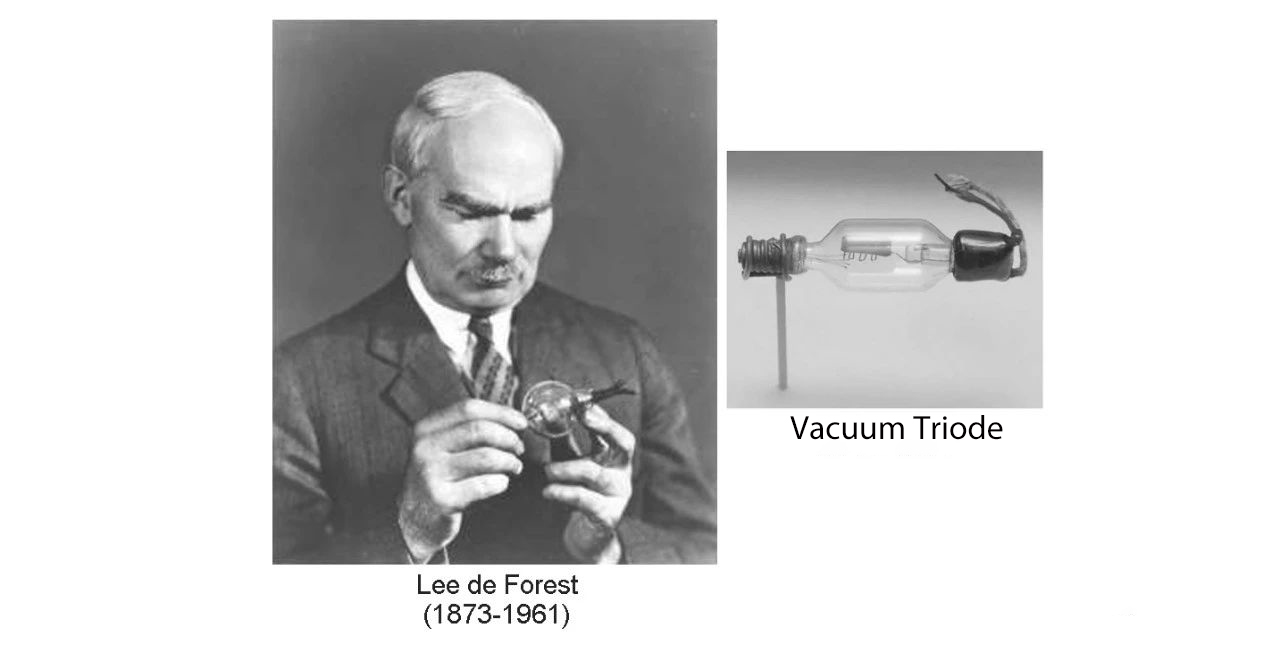
Figure 3. Forrester's invention of the vacuum triode
The vacuum triode is considered to be the starting point of the birth of the electronics industry. It was used for a period of more than 40 years. Due to the drawbacks of large size, power consumption and poor reliability of the electron tube, it was eventually replaced by the later transistor.
3. Invention of the transistor (1947, 74 years ago)
In 1947, J. Bardeen, W. Brattain, and W. Shockley of Bell Laboratories invented the point contact transistor, an NPN germanium (Ge) transistor, for which the three of them won the 1956 Nobel Prize in Physics.
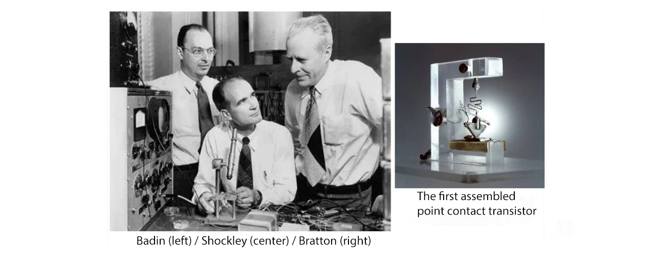
Figure 4. The trio of transistor inventions
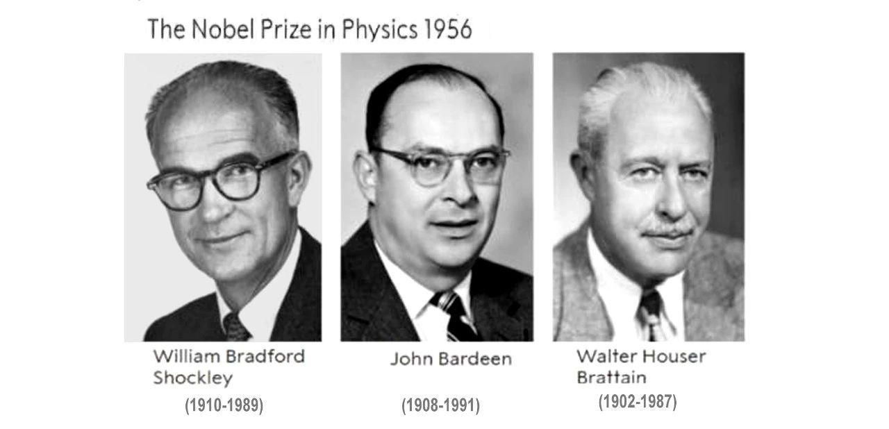
Figure 5. The trio that won the 1956 Nobel Prize in Physics
In 1950, when G.K. Teal and J.B. Little succeeded in the process of growing large single-crystal germanium, William W. Shockley made the first bipolar junction transistor, the PN junction transistor, in April 1950. W. Shockley made the first bipolar junction transistor, the PN junction transistor, in April 1950, which was much more widely used in practice than the point contact transistor. Most of the transistors today are still PN junction transistors. The so-called PN junction is the combination of P-type semiconductor and N-type semiconductor, where P-type semiconductor has more holes and N-type semiconductor has more electrons.
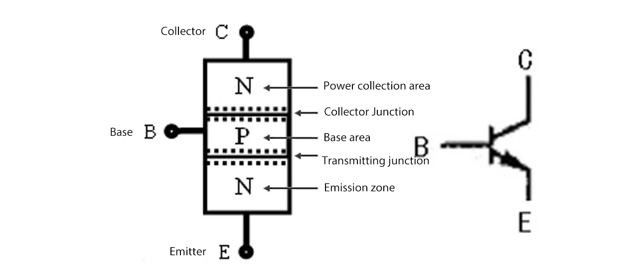
Figure 6. PN junction transistor structure schematic (left) transistor symbol (right)
In 1952, the practical JunctionField-Effect Transistor (JFET) was manufactured. The Junction Field-Effect Transistor (JFET) is a transistor that uses the electric field effect to control the current. In 1960, silicon dioxide was proposed to improve the performance of bipolar transistors, and the Metal Oxid Semiconductor (MOS) field-effect transistor was born. M. Atalla is also credited as one of the inventors of the MOS field-effect transistor (MOSFET).
MOSFETs proclaimed their dominance in electronics and underpinned the development of large-scale integrated circuits, the cornerstone of today's information society. In fact, the field effect transistor (FET) was developed by Julius Lillingfeld. Julius Lilienfeld and German physicist Oskar Heil in 1925. Heil (Oskar Heil) in 1934, respectively, but has not been able to manufacture practical transistor devices.
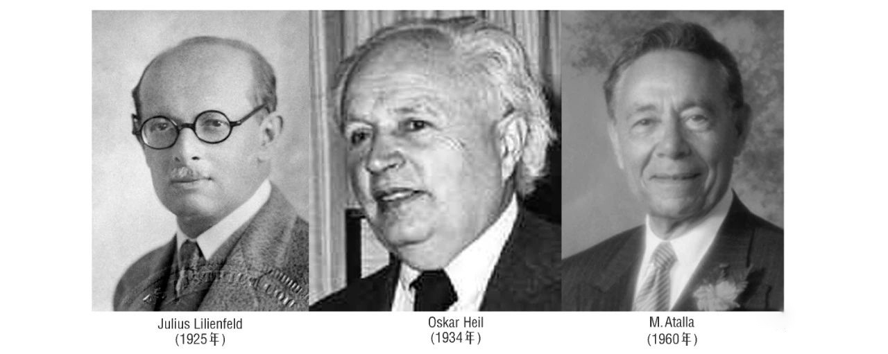
Figure 7. Contributors to the invention of MOSFETs and the year of invention
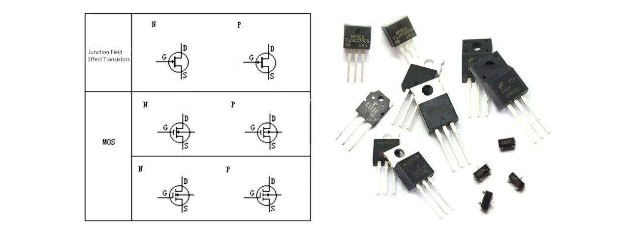
Figure 8. Field effect transistor (FET) classification and physical diagram
Transistors range from bipolar type to MOS type, from discrete devices to integrated in chips, and with the different semiconductor materials they use, there are many types and varieties of transistors. Transistors mainly play the role of small signal amplification, power amplification, current switching, etc. It is the most basic circuit component with the largest number of integrated in the chip.
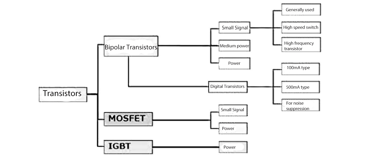
Figure 9. Classification of various transistors
The invention of the transistor was the first milestone in the development of microelectronics technology. The invention of the transistor brought mankind into the era of rapidly developing electronic information. Up to now, it has been used for 74 years.
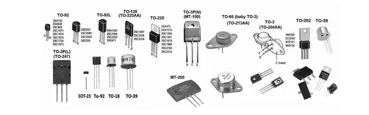
Figure 10. Discrete transistors in various package forms
4. The invention of integrated circuit (chip) (1958, 63 years ago)
In 1950, the American Russell Ohl and William O. Russell Ohl and William Shockley invented the ion implantation process. Shockley (W. Shockley) invented the ion implantation process, and in 1954 Shockley applied for a patent for this invention. Ion injection is the ionization of impurities into ions and focused into ion beams, accelerated in an electric field and injected into the silicon material to achieve the doping of silicon materials, the purpose is to change the conductive properties of silicon materials. Ion injection is the earliest adopted method for semiconductor doping, and it is one of the basic processes for chip manufacturing.
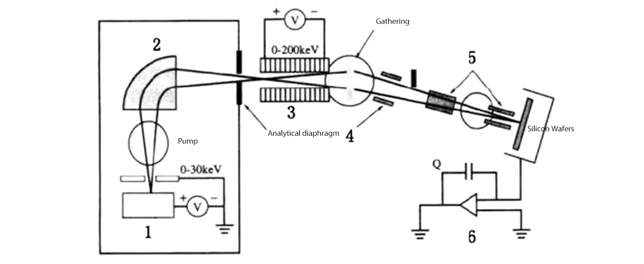
Figure 11. A brief schematic of the ion implantation principle
In 1956, C.S. Fuller, an American, invented the diffusion process; diffusion is another method of doping, and it is also one of the basic processes for chip fabrication.

Figure 12. Schematic diagram of a thermal diffusion device
The ion injection process and the diffusion process are two doping methods. Ion injection is used to form shallow semiconductor junctions (Junctions) and diffusion is used to form deeper semiconductor junctions. Doping is like adding seasoning to a stir-fry, it is the "spicing up" of the semiconductor material. A small amount of other substances mixed into the very pure semiconductor material, so that it becomes impure, for semiconductor materials, other substances are impurities, the process of doping is called doping. Doping is the process of adding a certain amount of other substances to a semiconductor material to artificially change the electrical properties of the semiconductor material.
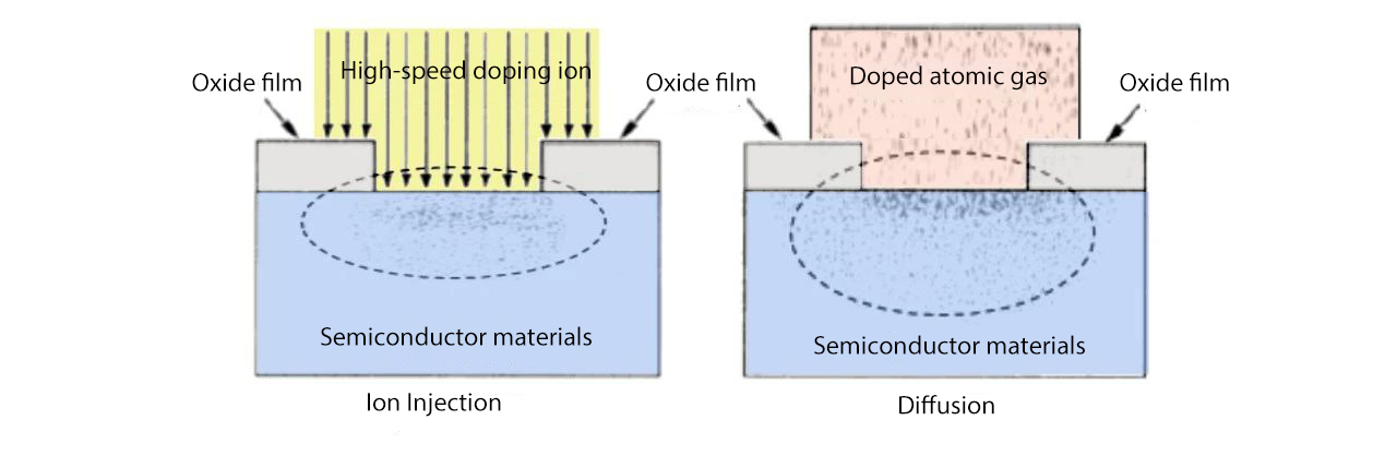
Figure 13. Schematic diagram of two types of semiconductor doping
In 1958, Robert Noyce of Centron Inc. In 1958, Robert Noyce of Centron Inc. and Jack Kilby of DEI Inc. In 1958, Robert Noyce of Centron and Jack Kilby of DEI invented the integrated circuit a few months apart, starting the history of microelectronics in the world. Based on Kilby's invention, Noyce invented the commercially available integrated circuit, bringing the semiconductor industry from the "invention era" to the "commercial era".
Kilby was awarded the Nobel Prize in Physics in 2000 for his invention of the integrated circuit. Noyce, one of the founders of Centron Semiconductor (founded in 1957) and Intel Corporation (founded in 1968), was a great scientist and an important figure in the history of integrated circuits. Unfortunately, his previous work in the Shaw Clay Laboratory, the invention of "negative resistance diode" was not supported by the boss and terminated, and later the Japanese scientist Leo Esaki (Esaki) on this invention won the Nobel Prize; he died in 1990, did not wait until 2000 to share the year with Kilby Nobel Prize in Physics, both times with the highest honors in science and technology. However, both are considered to be the fathers of the integrated circuit.
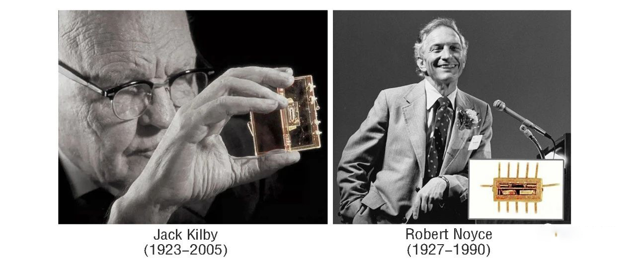
Figure 14. Kilby and Noyce with their chip inventions
In 1959, Korean-born scientists Dawon Kahng and Martin M. Ettalla of Bell Labs were awarded the prize for their invention of the chip. Martin M. Atalla invented the Metal-Oxide-Semiconductor Field-Effect Transistor (MOSFET), which was the first truly compact MOSFET and the first transistor that could be miniaturized and actually produced. The MOSFET had a profound impact on the development of the electronics industry.
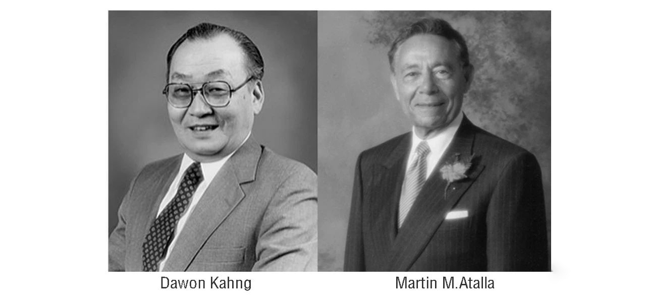
Figure 15.Jiang Ohara and Ettala invented the MOSFET
5. Photolithography is the soul of chip manufacturing (invented 61 years ago)
In 1960, Loor (H.H. Loor) and Christenson (Christenson) invented the epitaxial process. Epitaxy refers to the growth of a single crystal layer on a semiconductor single crystal material with certain requirements and in the same crystal orientation as the substrate, as if the original crystal had been extended outward.
Was the photolithography process first used in chip manufacturing in 1960? This is an important question that needs to be focused on in this paper. Another article in my public website [Core Talk], "How did lithography turn into a chip manufacturing neck technology step by step?" pointed out that lithography is the soul technology of chip manufacturing. It is the emergence of photolithography that has brought silicon device manufacturing into the era of planar processing technology and the rapid development of large-scale integrated circuits and microelectronics today.
The invention of photolithography in a general sense should be traced back to the French scientist Joseph Netherford in 1822. Netherford. Joseph Nicephore Niepce's experiments on photographic materials and etching, and his replica of the d'Amboise bishop's statue made in 1827. The photolithography process in this paper refers specifically to the photolithography process technology in the chip manufacturing process.
When exactly was the lithography process for chip manufacturing invented? I found that there are few articles on the Internet in this regard, and even if there are articles about it, they are all in passing. The first statement is that the photolithography process was invented by H.H. Loor and E. Castellani in 1960 . The second statement is that the lithography process was invented by E. Spiller and E. Castellani in 1970 . The time difference between the invention of lithography in the two statements is as long as 10 years. It is also difficult to find out how Lohr, Castellani and Spiller invented lithography on the Internet, or even their biographies.
I believe that 1960 should be the year of the invention of lithography. Because, if the photolithography process was only invented in 1970, it would have been difficult to manufacture semiconductor products (bipolar, FET, MOSFET transistors) and chips from pioneering companies such as Bell Labs, Fairchild, TI, RCA and Intel in the decade or so from 1958 to 1970.
The author also believes that Fairchild should be the place where the lithography process was invented. 1958 several founders of Fairchild bought three 16mm lenses from a camera store, made a step and repeat photographic device to make masks, and improved the mask plates, photoresist. 1959, Robert Noyce (RCA), the founder of Fairchild, was the inventor of the lithography process. Noyce (Robert Noyce) proposed a technical idea in his diary, "If you can make individual transistors by photolithography, why can't you make transistors in bulk by photolithography?" , "Putting multiple components on a single wafer would enable the internal connection of components in the process, which would reduce size and weight, and lower the price." For this reason, Fairchild began to experiment with the lithography process for transistor volume manufacturing. Noyce proposed the idea of "planar technology," and Jean Hoerer (Jean Hoerer), who was a member of the board of directors of the company, was a member of the board. Jean Hoerni was the one who transformed this idea into a practical "planar processing" technology .
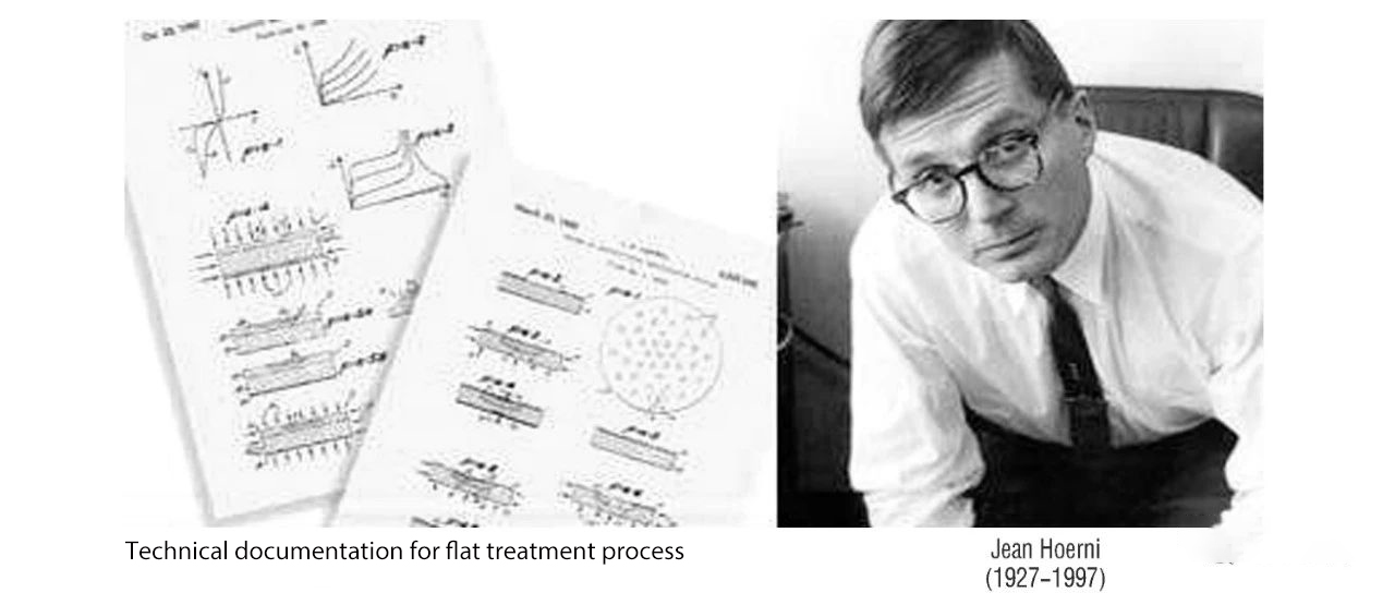
Figure 17. Hoerni and the technical documentation of the planar processing process
From the development of photolithography, in the 1960s it was contact lithography and proximity lithography; in the 1970s it was projection lithography; in the 1980s it was stepper lithography; and then stepper scanning lithography, immersion lithography and now EUV lithography , it is clear that the lithography process for chip manufacturing could not have been invented only in 1970.
Process technologies such as ion injection, diffusion, epitaxy, and lithography, together with vacuum coating technology, oxidation technology, and test packaging technology, constitute the main body of silicon planar processing technology and, in layman's terms, the main body of chip manufacturing. Without lithography technology, there would be no chip technology and industry today, and there would be no information and intelligent society now.
6. Chip technology continues to mature and develop rapidly along Moore's Law
In 1962, Steven Hofstein of Radio Corporation of America (RCA) was the founder of the company. Hofstein (Steven Hofstein) Frederic Heimann (Frederic Heimann) Heiman (Frederic Heiman) developed a mass-produced metal oxide semiconductor field effect transistor MOSFET, and the use of experimental 16 MOS transistors integrated into a chip, which is the world's first MOS integrated circuit in the true sense.

Figure 18. Hofstein and the world's first MOS integrated circuit
In 1963, Frank M. Wanrath of Centron Inc. Wanlass (Frank M. Wanlass) and Chinese Saatchi Tang (C.T. Sah) first proposed CMOS circuit technology. They connected N-MOS and P-MOS in a complementary structure, with one MOSFET off and one MOSFET on for both polarities, with almost no quiescent current, suitable for logic circuits. in June 1963, Wanlass applied for a patent for CMOS, but he left Fairchild a few days later. The first CMOS circuit chip was developed by RCA. CMOS circuit technology laid a solid foundation for the development of large-scale integrated circuits. Today, more than 95% of all integrated circuit chips are manufactured on the basis of CMOS processes.
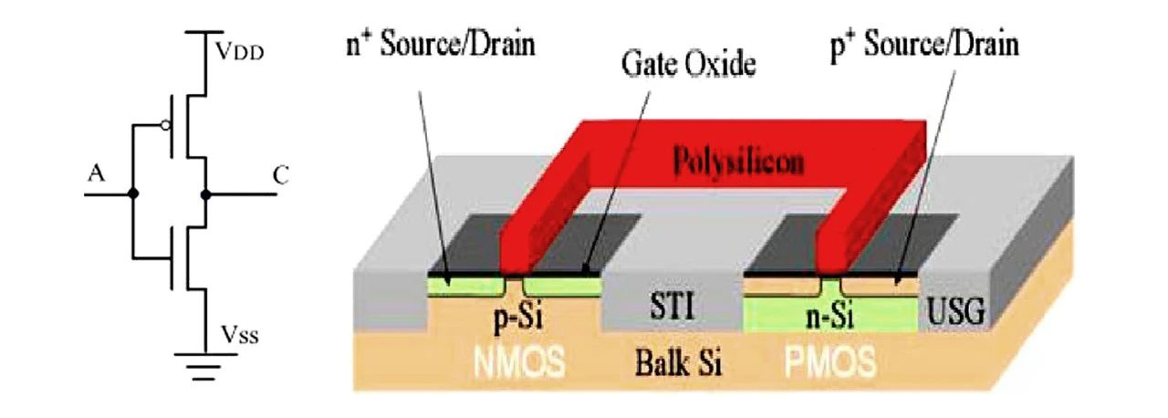
Figure 19. CMOS inverter circuit symbol and device model
In the same year, Robert Widlar, a 26-year-old circuit design prodigy at Centron, was born. Robert Widlar designed the first integrated operational amplifier circuit, the µA702.
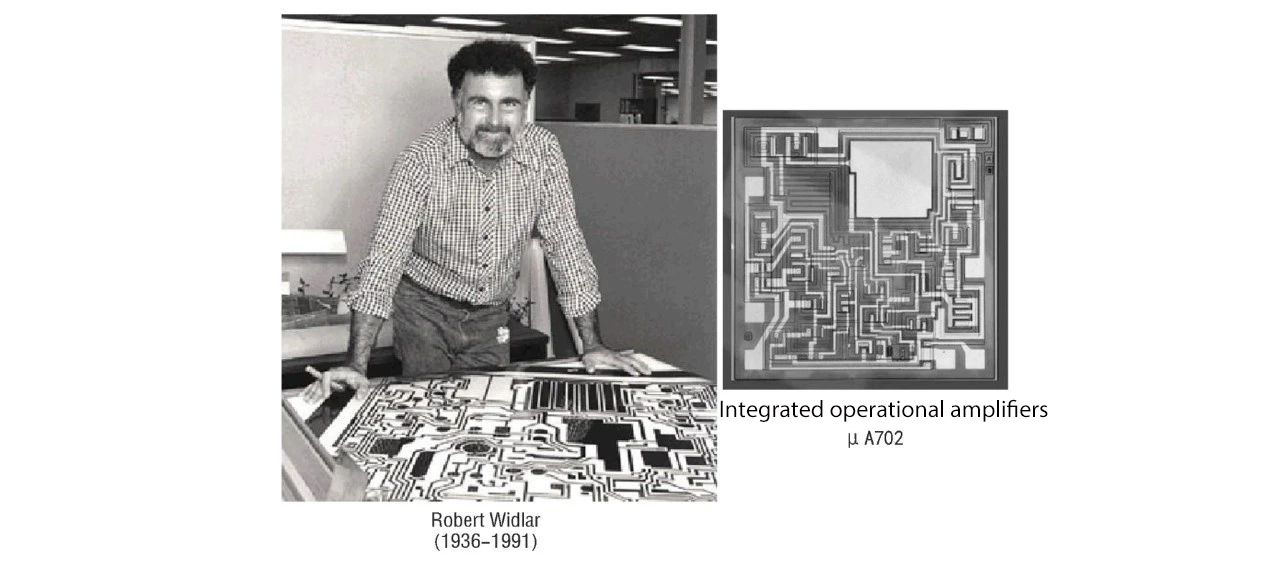
Figure 20. μA702 op-amp chip from Centson
In 1964, Gordon Moore, one of the founders of Intel Corporation, designed the µA702 op-amp chip. Moore (Gordon Moore) proposed the famous Moore's Law (Moore's Law), predicting that the future trend of chip technology is that when the price remains the same, the number of components that can be accommodated on the chip, about every 18-24 months will double, and the performance will double. Later more than 50 years of chip technology development proved Moore's Law is still basically accurate.
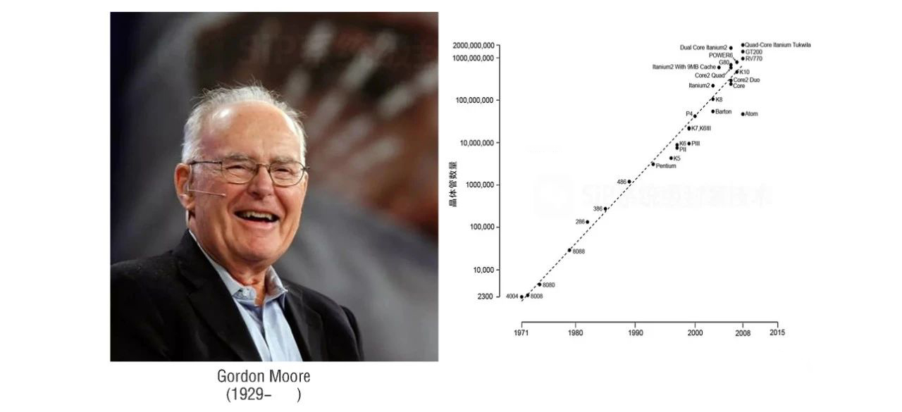
Figure 21. Moore, chip technology trends along Moore's law
In 1966, the U.S. company RCA developed CMOS integrated circuits and the first 50-gate gate array chip.
In 1967, the U.S. AppliedMaterials (AppliedMaterials) was founded, and has become the world's largest semiconductor equipment manufacturing company. fiscal year 2020 annual revenue of $ 17.2 billion, research and development investment of $ 2.2 billion, 24,000 employees worldwide, with 14,300 patents. The business covers semiconductor, display, solar, flexible coating, automation software, etc. The following chart is an overview of Applied Materials' semiconductor business segment.
In 1967, DawonKahng and Simon Sze invented non-volatile memory at Bell Labs. This is a floating-gate MOSFET, which is the basis for erasable programmable read-only memory (EPROM), electrically erasable programmable read-only memory (EEPROM), and flash memory (Flash).
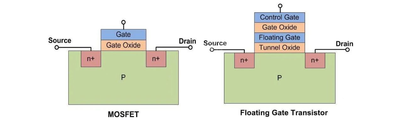
Figure 23. Schematic diagram of a normal MOSFET and a floating-gate MOSFET
In 1968, Robert H. Dennard of IBM Corporation Robert H. Dennard of IBM invented the single-transistor dynamic random access memory (DRAM). The name of the invention was "An Invention of a Transistorized Dynamic RAM Cell". Dennard was inducted into the National Inventors Hall of Fame in 1997 and received the IEEE Medal of Honor in 2009, the highest honor in the electrical and electronics field.
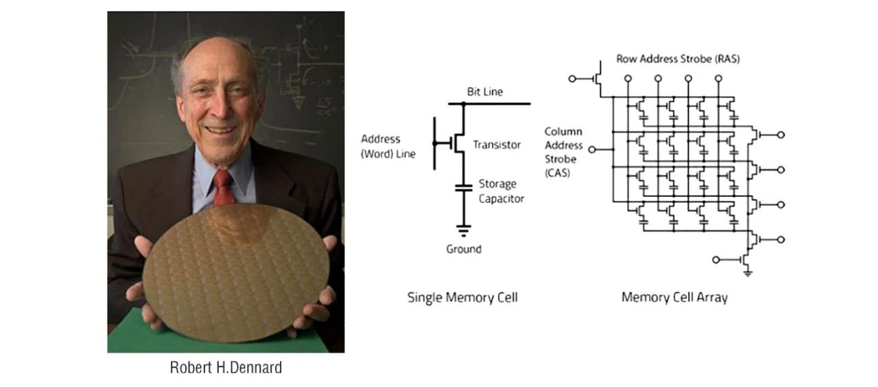
Figure 24. Schematic of Dennard with single-transistor DRAM
Unfinished business to be continued.
Stay tuned: The 60+ year history of chip technology in pictures (middle part).


Phone:+86-137-5112-7429
Email:sales@hyx-tech.com
Address:14D2, block A, Modern window building,ZhenHua Road,Futian District, Shenzhen
 sales@hyx-tech.com
 +86-0755-2399-7487
 sales@hyx-tech.com
 Login
Login Register